Electro-optic phase shifter doping structure, preparation method and electro-optic modulator

A phase shifter, electro-optical technology, applied in instruments, optics, nonlinear optics, etc., can solve the problem that the interdigitated doping structure increases the total area of ​​the PN junction, which is unfavorable for low-cost mass production, and the dynamic power consumption of the modulator increases. and other problems, to achieve the effect of improving the phase-shifting efficiency, reducing the processing accuracy, and reducing the modulation bandwidth.

Active Publication Date: 2022-03-25
HUAZHONG UNIV OF SCI & TECH
View PDF5 Cites 0 Cited by
  • Summary
  • Abstract
  • Description
  • Claims
  • Application Information

AI Technical Summary

Problems solved by technology

The interdigitated doping structure increases the total area of ​​the PN junction, which significantly increases the junction capacitance of the phase shifter while improving the phase shifting efficiency, resulting in an increase in the dynamic power consumption and a decrease in the electrical bandwidth of the modulator.
In addition, in order to take both modulation efficiency and modulation bandwidth into consideration, a PN junction with L-type doping distribution appears in related technologies. This kind of PN junction is easy to form extremely high series resistance due to the alignment error between the doped mask and the optical waveguide. As a result, the electrical bandwidth of the modulator deteriorates significantly, which requires high processing precision and low yield, which is not conducive to low-cost mass production

Method used


Image

  • Electro-optic phase shifter doping structure, preparation method and electro-optic modulator
  • Electro-optic phase shifter doping structure, preparation method and electro-optic modulator
  • Electro-optic phase shifter doping structure, preparation method and electro-optic modulator

Examples


Embodiment Construction

[0030] In order to make the object, technical solution and advantages of the present invention clearer, the present invention will be further described in detail below in conjunction with the accompanying drawings and embodiments. It should be understood that the specific embodiments described here are only used to explain the present invention, not to limit the present invention. In addition, the technical features involved in the various embodiments of the present invention described below can be combined with each other as long as they do not constitute a conflict with each other.

[0031] In the present invention, the terms "first", "second" and the like (if any) in the present invention and drawings are used to distinguish similar objects, and are not necessarily used to describe a specific order or sequence.

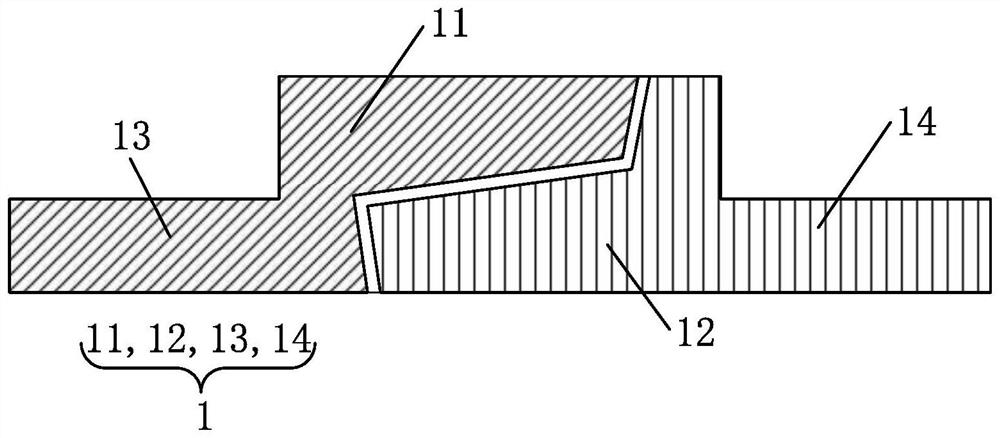
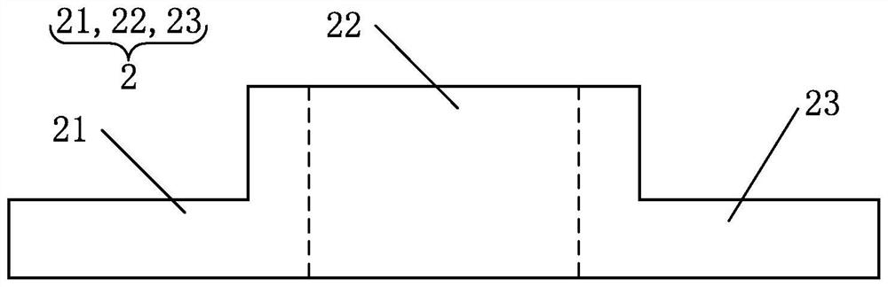
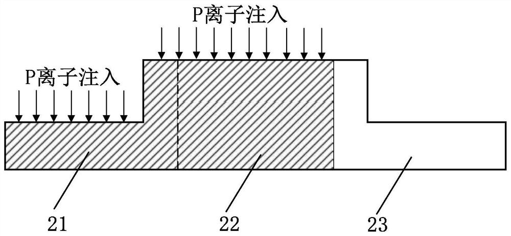
[0032] refer to figure 1 , the doping structure of the electro-optic phase shifter in this embodiment (hereinafter simply referred to as the doping structure) wil...


PUM


Abstract

The invention discloses an electro-optic phase shifter doping structure, a preparation method and an electro-optic modulator, belonging to the field of semiconductor optoelectronic devices. The electro-optic phase shifter doping structure includes a ridge-shaped optical waveguide, and the ridge-shaped optical waveguide includes a ridge region and a The rib regions on both sides of the region, the ridge region includes an N-type doped ridge region and a P-type doped ridge region, and two vertically inclined PN junctions and connections are formed at the interface between the N-type doped ridge region and the P-type doped ridge region. The laterally inclined PN junction of the two vertically inclined PN junctions; wherein, the interface between the N-type doped ridge region and the P-type doped ridge region does not intersect the left and right sides of the ridge region. The doping structure in the present invention increases the overlapping area of ​​the optical field and the PN junction in the phase shifter, improves the phase shifting efficiency, has a lower driving voltage, reduces the power consumption of the phase shifter, and has an impact on the modulation bandwidth of the phase shifter Very small, compatible with CMOS process and has a large process tolerance, thus ensuring the yield rate of the device.

Description

technical field [0001] The invention belongs to the field of semiconductor optoelectronic devices, and more specifically relates to an electro-optic phase shifter doping structure, a preparation method and an electro-optic modulator. Background technique [0002] Optical modulators have the advantages of high speed, low power consumption, and low cost, and have attracted extensive attention in the field of communication. Electro-optic modulators based on silicon-optical platforms are currently commonly used electro-optic modulators. The electro-optic phase shifter is an important part of the electro-optic modulator, and its performance directly determines the power consumption and modulation rate of the electro-optic modulator. The optical waveguide of the electro-optical phase shifter is doped to form a PN junction. When the external reverse bias voltage changes, the area of ​​the PN junction changes, causing the effective refractive index of the optical waveguide to chang...

Claims


Application Information

Patent Timeline
Patent Type & Authority Patents(China)
IPC IPC(8): G02F1/025
CPCG02F1/025
Inventor 余宇付思东
Owner HUAZHONG UNIV OF SCI & TECH
Why Eureka
Try Eureka