Spin electronic device, SOT-MRAM storage unit, storage array and storage and calculation integrated circuit

A technology for spintronic devices and memory cells, which is applied in the direction of electric solid devices, circuits, electrical components, etc., can solve the problems that the spin-orbit moment cannot be magnetized and cannot be reversed and cannot realize the integrated application of CMOS technology, and is conducive to large-scale preparation and integration. Application and realization of the effect of the integrated function of storage and calculation

Pending Publication Date: 2020-11-27
INST OF MICROELECTRONICS CHINESE ACAD OF SCI
View PDF3 Cites 7 Cited by
  • Summary
  • Abstract
  • Description
  • Claims
  • Application Information

AI Technical Summary

Problems solved by technology

[0004] What the present invention aims to solve is the problem that the existing spin-orbit moment cannot complete the deterministic magnetization reversal under the condition of no external magnetic field and cannot realize the integrated application compatible with the existing CMOS process

Method used


Image

  • Spin electronic device, SOT-MRAM storage unit, storage array and storage and calculation integrated circuit
  • Spin electronic device, SOT-MRAM storage unit, storage array and storage and calculation integrated circuit
  • Spin electronic device, SOT-MRAM storage unit, storage array and storage and calculation integrated circuit

Examples


Embodiment Construction

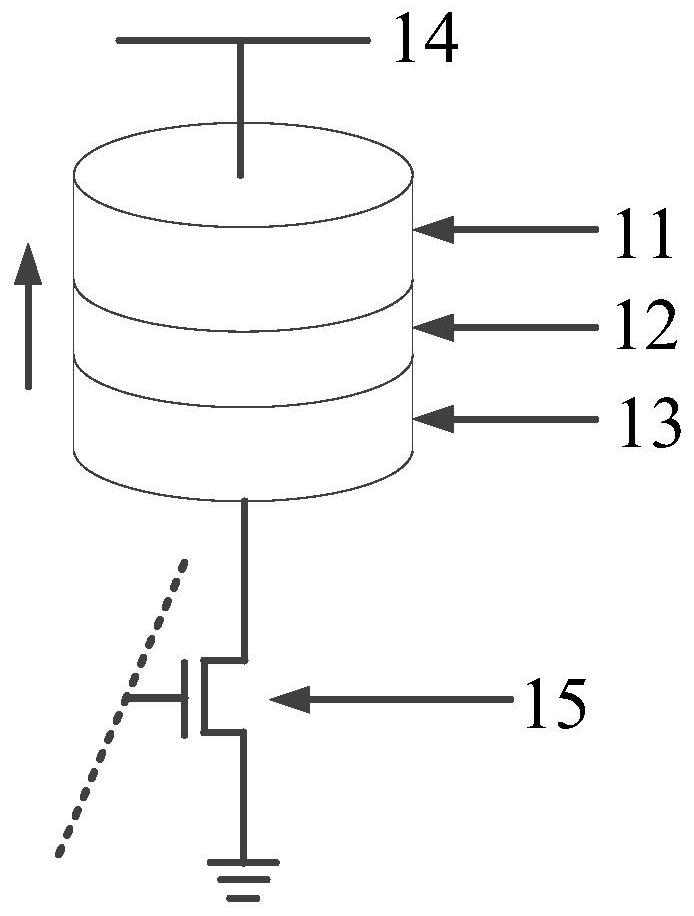
[0059] figure 1 It is a structural schematic diagram of an existing STT-MRAM memory cell, the STT-MRAM memory cell includes a gate transistor 12 and a magnetic tunnel junction arranged between a bit line 11 and a word line 12, and the magnetic tunnel junction includes a stacked arrangement Reference layer 14 , insulating layer 15 and free layer 16 . When the gate transistor 13 is turned on, the magnetic tunnel junction is turned on, and the electrons in the bit line 11 are injected into the reference layer 14 to generate a spin current with the same polarization direction as that of the reference layer 14 . The spin current jumps through the insulating layer 15, and transfers the spin torque to the free layer 16, so that the magnetization direction of the free layer 16 is reversed to be the same as that of the reference layer 14. At this time, the The magnetic tunnel junction presents a low-resistance state, achieving the purpose of writing binary data "0". When a current i...


PUM


Abstract

The invention discloses a spin electronic device, an SOT-MRAM storage unit, a storage array and a storage and calculation integrated circuit. The spin electronic device comprises a ferroelectric / ferromagnetic heterostructure, a magnetic tunnel junction and a heavy metal layer arranged between the ferroelectric / ferromagnetic heterostructure and the magnetic tunnel junction. The ferroelectric / ferromagnetic heterostructure comprises a multiferroic material layer and a ferromagnetic layer which are arranged in a stacked mode, the magnetic tunnel junction comprises a free layer, an insulating layerand a reference layer which are arranged in a stacked mode, and the heavy metal layer is arranged between the ferromagnetic layer and the free layer. According to the spin electronic device, the SOT-MRAM storage unit, the storage array and the storage and calculation integrated circuit, deterministic magnetization overturning under the condition of no external field assistance can be realized.

Description

technical field [0001] The invention relates to the technical field of integrated circuits, in particular to a spintronic device, a SOT-MRAM memory unit, a memory array, and a memory-computing integrated circuit. Background technique [0002] Among many new non-volatile memories, spintronic devices have the advantages of high speed, low energy consumption, anti-fatigue, anti-radiation, and easy miniaturization, making them attract worldwide attention in the field of information. A magnetic random access memory (MRAM, Magnetic Random Access Memory) based on a magnetic tunnel junction (MTJ, Magnetic Tunnel Junction) is the most concerned type of spintronic device. The second-generation MRAM that is currently being vigorously developed is realized by using the spin transfer torque (STT, Spin Transfer Torque) effect. The information writing process of STT-MRAM requires a large current to pass through the magnetic tunnel junction, so the information writing process is accompanied...

Claims


Application Information

Patent Timeline
Patent Type & Authority Applications(China)
IPC IPC(8): H01L27/22H01L43/08H01L43/10
CPCH10B61/22H10N50/85H10N50/10G11C11/1675G11C11/22G11C11/1659G11C11/1655G11C11/1657G11C8/16G11C11/1673G11C11/161H10N50/80
Inventor 邢国忠林淮路程刘琦吕杭炳李泠刘明
Owner INST OF MICROELECTRONICS CHINESE ACAD OF SCI
Why Eureka
Try Eureka