Device and method for placing chip on jumper frame

A frame and chip technology, applied in the field of chip placement devices, can solve the problems of difficult attachment of IC chips, reduced patch quality, and reduced fluidity of solder paste, so as to shorten the overall process time, prevent solder paste from solidifying, and improve packaging quality. Effect

Active Publication Date: 2020-12-01
四川旭茂微科技有限公司
View PDF14 Cites 6 Cited by
  • Summary
  • Abstract
  • Description
  • Claims
  • Application Information

AI Technical Summary

Problems solved by technology

[0005] In the packaging process, the IC chip needs to be attached to the jumper frame through solder paste, that is, the patch process. Before the patch, the corresponding solder paste needs to be applied to the jumper frame, that is, the tin spray process. The SMT process and the tin sprayi

Method used


Image

  • Device and method for placing chip on jumper frame
  • Device and method for placing chip on jumper frame
  • Device and method for placing chip on jumper frame

Examples


Embodiment Construction

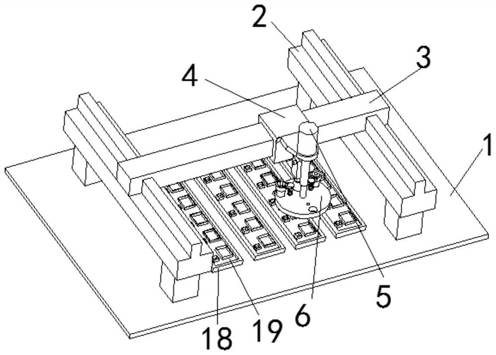
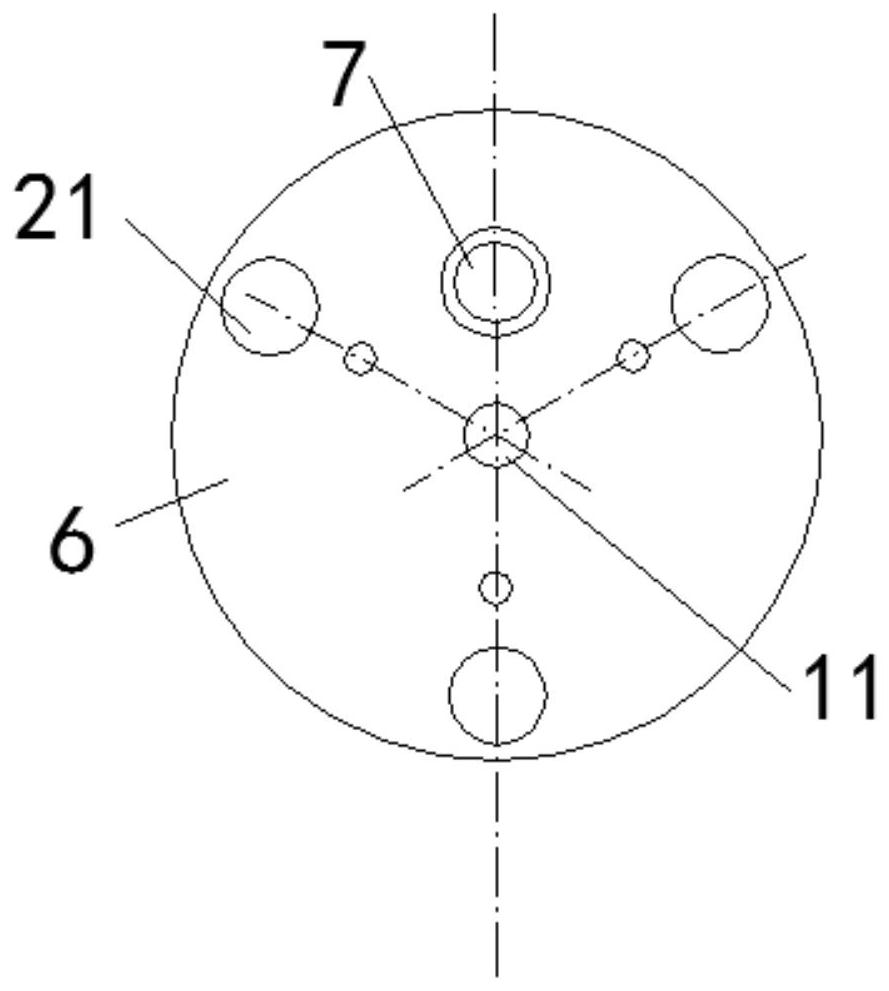
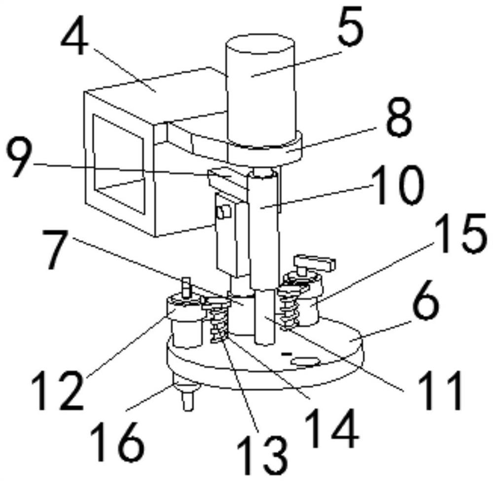
[0039] The following will be combined with Figure 1-8, clearly and completely describe the technical solutions of the present invention, and obviously, the described embodiments are part of the embodiments of the present invention, but not all of them. Based on the embodiments of the present invention, all other embodiments obtained by persons of ordinary skill in the art without making creative efforts belong to the protection scope of the present invention.

[0040] In the description of the present invention, it should be understood that the orientation or positional relationship indicated by the terms "upper", "lower", "front", "rear", "inner", "outer" etc. Orientation or positional relationship is only for the convenience of describing the present invention and simplifying the description, and does not indicate or imply that the referred device or element must have a specific orientation, be constructed and operated in a specific orientation, and thus should not be const...


PUM


Abstract

The invention discloses a device and a method for placing a chip on a jumper frame. The device comprises a sliding block, a motor, a disc, an electric cylinder, a solder paste spraying gun, a vacuum adsorption device, a reset mechanism, a translation frame and a placing mechanism, wherein one side of the sliding block is connected with the motor; the output shaft of the motor is connected with thedisc; the disc is provided with three placing holes; the solder paste spraying gun and the vacuum adsorption device are respectively arranged in the two placing holes in an up-and-down sliding manner; the electric cylinder is used for driving the solder paste spraying gun and the vacuum adsorption device to slide; the reset mechanism is used for resetting the solder paste spraying gun and the vacuum adsorption device; the translation frame is connected with the sliding block for driving the sliding block to slide longitudinally or transversely; the placing mechanism is arranged on the workingtable and used for positioning and placing the IC chip and the jumper frame. The technical problems in the prior art are solved, for example, the tin spraying process and the chip mounting process are separately carried out, so that IC chip adsorption and chip mounting quality are easily affected.

Description

technical field [0001] The invention relates to the field of chip packaging, in particular to a chip placement device and method on a wire jumper frame. Background technique [0002] IC chip (Integrated Circuit Chip) is an integrated circuit formed by placing a large number of microelectronic components (transistors, resistors, capacitors, etc.) on a plastic base to make a chip. IC chips include wafer chips and packaged chips, and the corresponding IC chip production line consists of two parts: a wafer production line and a packaging production line. [0003] The jumper is the lead wire, and the jumper frame is the lead frame. As the chip carrier of the integrated circuit, it is a kind of electrical connection between the lead-out end of the chip's internal circuit and the outer lead by means of bonding materials (gold wire, aluminum wire, copper wire). The key structural part that forms the electrical circuit, it acts as a bridge connecting the external wires, most of the ...

Claims


Application Information

Patent Timeline
IPC IPC(8): H01L21/68H01L21/683H01L21/67H01L21/60
CPCH01L21/67144H01L21/6715H01L21/67155H01L21/6838H01L21/68H01L21/67276H01L24/81H01L2224/81986H01L2224/81024H01L2224/818H01L2224/8112
Inventor 赵雪贺国东王秋明贺姣
Owner 四川旭茂微科技有限公司
Why Eureka
Try Eureka