

Polishing method for gallium antimonide monocrystal wafer
A single-wafer, gallium antimonide technology, applied in polishing compositions containing abrasives, grinding/polishing equipment, grinding/polishing safety devices, etc., can solve the problem of many operation steps, complicated polishing process, and easy introduction of surface defects and other problems, to achieve the effect of simple process, low surface roughness and good stability
- Summary
- Abstract
- Description
- Claims
- Application Information
AI Technical Summary
Problems solved by technology
Method used
Image

Examples
Embodiment 1
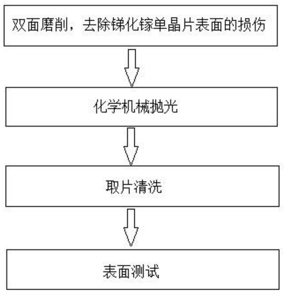
[0033] (1) Remove the damage on the surface of the gallium antimonide single wafer; paste the gallium antimonide single wafer evenly on the ceramic carrier with quartz wax and use natural curing, wipe off the excess quartz wax with alcohol, and then pass it through the grinding machine Use 6000 mesh grinding wheel, 4000 rpm for double-sided grinding, and the removal amount is controlled to 40um.
[0034] (2) Chemical mechanical polishing: the polishing cloth is made of black synthetic leather, the length of the polishing cloth is 225um, and the aperture of the polishing cloth is 50-90um.
[0035] The polishing liquid is made by mixing the following components according to the mass percentage: 50nm SiO 2 1.2% suspended abrasive, 0.5% sodium dichloroisocyanurate, 2% sodium bicarbonate, 0.25% sodium pyrophosphate, 0.25% sodium benzenesulfonate, and the balance is deionized water.
[0036] The process parameters of the polishing process are as follows: the polishing pressure is 2...
Embodiment 2
[0040] The polishing process of the gallium antimonide single wafer provided in this embodiment is basically the same as that of the above-mentioned embodiment 1, except that the length of the polishing cloth is 350 um, and the diameter of the polishing cloth is 30-70 um.
[0041] The polishing liquid is made by mixing the following components according to the mass percentage: 50nm SiO 2 1.2% suspended abrasive, 0.25% sodium dichloroisocyanurate, 2% sodium bicarbonate, 0.25% sodium pyrophosphate, 0.25% sodium benzenesulfonate, and the balance is deionized water.
[0042] The process parameters of the polishing process are as follows: the polishing pressure is 200g / cm 2 , the polishing speed is 40-100 rpm, the flow rate of the polishing liquid is 30mL / min, and the polishing time is 50min.
Embodiment 3
[0044] The polishing process of the gallium antimonide single wafer provided in this embodiment is basically the same as that of the above-mentioned embodiment 1, except that the length of the polishing cloth is 225um, and the diameter of the polishing cloth is 50-90um.
[0045] The polishing liquid is made by mixing the following components according to the mass percentage: 50nm SiO 2 1.2% suspended abrasive, 0.25% sodium dichloroisocyanurate, 2% sodium bicarbonate, 0.25% sodium pyrophosphate, 0.25% sodium benzenesulfonate, and the balance is deionized water.
[0046] The process parameters of the polishing process are as follows: the polishing pressure is 200g / cm 2 , the polishing speed is 70 rpm, the flow rate of the polishing solution is 30mL / min, and the polishing time is 50min.
PUM
| Property | Measurement | Unit |
|---|---|---|
| particle diameter | aaaaa | aaaaa |
| surface roughness | aaaaa | aaaaa |
| surface roughness | aaaaa | aaaaa |
Abstract
Description
Claims
Application Information