Automatic high-precision tin soldering device for printed circuit board processing

A printed circuit board, automated technology, applied in the field of electronic parts processing, can solve the problems of weak welding, poor solder joint formation, virtual welding, etc., which is beneficial to daily maintenance, quick and easy assembly and positioning, and reduces use costs. Effect

Inactive Publication Date: 2020-12-15
东莞市优伟机电科技有限公司
View PDF0 Cites 1 Cited by
  • Summary
  • Abstract
  • Description
  • Claims
  • Application Information

AI Technical Summary

Problems solved by technology

[0003] The common problems of the existing automatic soldering equipment for printed circuit boards are: the problems of the automatic soldering machine are mainly manifested in the phenomenon of low precision of solder joints, virtual soldering, continuous soldering, stacking tin, sharpening, and missing soldering, etc., specifically: virtual Welding generally refers to the fact that the solder joints seem to be okay during the welding process, but in fact the welding is not firm or the amount of tin penetration is not enough; continuous welding generally refers to the phenomenon that several adjacent solder joints stick together during the soldering process; Tin accumulation generally means that the solder joints are welded into a spherical shape, and the pin legs do not leak out; leakage soldering generally refers to the phenomenon that there is no tin on the pad during the welding process of the automatic soldering machine; Unsmooth and sharp points refer to the phenomenon that the solder joints are not well formed after welding or have burrs and sharp points

Method used


Image

  • Automatic high-precision tin soldering device for printed circuit board processing
  • Automatic high-precision tin soldering device for printed circuit board processing
  • Automatic high-precision tin soldering device for printed circuit board processing

Examples


Embodiment Construction

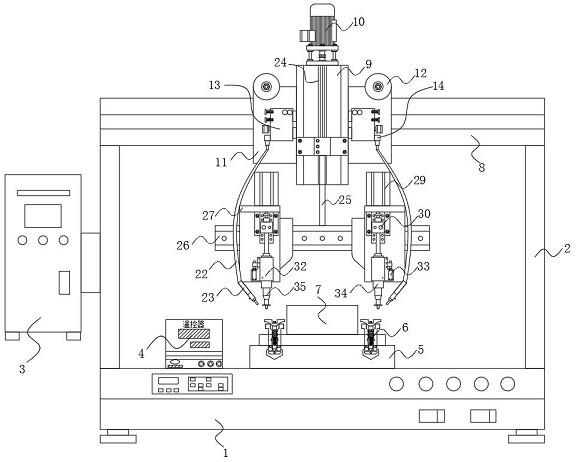
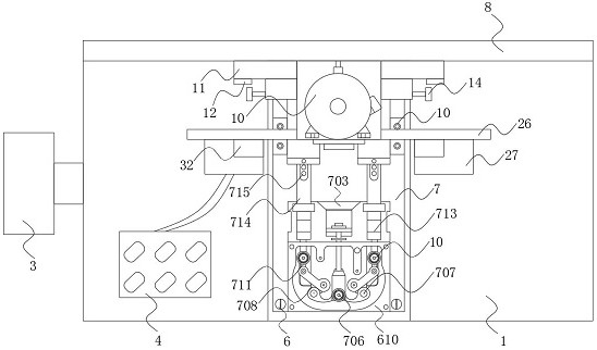
[0028] The following will clearly and completely describe the technical solutions in the embodiments of the present invention with reference to the accompanying drawings in the embodiments of the present invention. Obviously, the described embodiments are only some, not all, embodiments of the present invention.

[0029] In the description of the present invention, unless otherwise stated, the meaning of "plurality" is two or more; the terms "upper", "lower", "left", "right", "inner", "outer" , "front end", "rear end", "head", "tail", etc. indicate the orientation or positional relationship based on the orientation or positional relationship shown in the drawings, and are only for the convenience of describing the present invention and simplifying the description, rather than Indicates or implies that the device or element referred to must have a particular orientation, be constructed and operate in a particular orientation, and therefore should not be construed as limiting the...


PUM


Abstract

The invention discloses an automatic high-precision tin soldering device for printed circuit board processing, and relates to the technical field of electronic part processing, in particular to a base, a spring pre-tightening clamping mechanism, a centering clamp, a throttle valve and a soldering bit, a support is fixed to the top end of the base, and the spring pre-tightening clamping mechanism is arranged on the surface of a workbench. The bottom end of the soldering mechanism is provided with universal joints, according to the automatic high-precision tin soldering device for printed circuit board processing, the spring pre-tightening clamping mechanism is arranged, the mechanism can rapidly and simply assembly and positioning based on a rapid change clamping mechanism of the workbench,the rotation handle can achieve positioning and clamping of the substrate, the substrate and a clamp body are rapidly changed, the installation time is short due to the detachable structure design ofthe rotation handle, so that a user can replace the knurls or the wrench plane conveniently according to the actual situation, the problems that in the traditional technology, replacement is troublesome, and repeated positioning precision is too poor are solved, and the device has the advantages of being convenient to use and rapid in replacement.

Description

technical field [0001] The invention relates to the technical field of electronic parts processing, in particular to an automatic high-precision soldering equipment for printed circuit board processing. Background technique [0002] At present, electronic products are gradually becoming thinner and lighter, and their replacement speed is also increasing, and the functional requirements for electronic products are becoming more and more abundant. PCB (Printed Circuit Board, printed circuit board) is an important electronic component of electronic products. The support body of electronic components and the carrier of electrical connection of electronic components have higher and higher requirements for signal integrity and product reliability, especially signal integrity has become a problem that must be concerned in high-speed digital PCB design, and signal incompleteness may The system outputs incorrect data, causing the circuit to work abnormally or even not work at all, an...

Claims


Application Information

Patent Timeline
Patent Type & Authority Applications(China)
IPC IPC(8): H05K3/34H05K3/00H05K13/00
CPCH05K3/0008H05K3/34H05K13/0015
Inventor 白云杨宇民伍凤婵
Owner 东莞市优伟机电科技有限公司
Why Eureka
Try Eureka