Flat Panel Phased Array Antenna

A phased array antenna and flat panel technology, which is applied to antennas, antenna arrays, antenna components, etc., can solve the problems of increased pressing times, high processing costs, and difficult processing, and achieves reduced antenna area and low processing costs , The effect of small processing difficulty

Active Publication Date: 2021-02-26
CHENGDU T-RAY TECH CO LTD
View PDF12 Cites 0 Cited by
  • Summary
  • Abstract
  • Description
  • Claims
  • Application Information

AI Technical Summary

Problems solved by technology

[0003] (1) From the perspective of splicing, due to the need for partitions on the PCB, some areas are not equipped with antenna radiation units, so the existing array is only suitable for the splicing method of 2×n, which is not conducive to arbitrary splicing and large array arrays. The reason is that the extra area of ​​the control and power supply unit will cause the antenna to fail to scan normally, and phenomena such as grating lobes will appear during scanning
[0004] (2) In addition, controlling the power supply area and connectors will increase the area of ​​the entire PCB board, and the size of the whole machine will also increase relatively when the array is spliced, which is not conducive to product miniaturization design;
[0005] (3) From a design point of view, the antenna and the control power supply unit are on the same PCB, which will increase the number of wiring layers, resulting in an increase in the number of laminations, greater processing difficulty, higher scrap rate, and higher processing costs

Method used


Image

  • Flat Panel Phased Array Antenna
  • Flat Panel Phased Array Antenna
  • Flat Panel Phased Array Antenna

Examples


no. 1 example

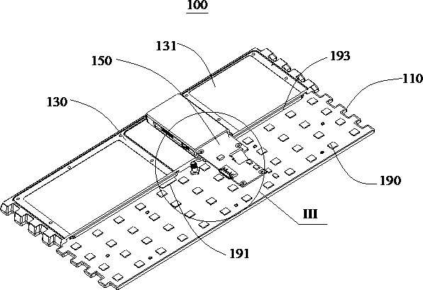
[0034]Please refer toFigure 1 to Figure 4The embodiment of the present invention provides a flat-panel phased array antenna 100, which can realize arbitrary splicing and large-array array, and has a small size, low processing difficulty, low processing cost, and convenient disassembly, maintenance or replacement.

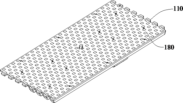
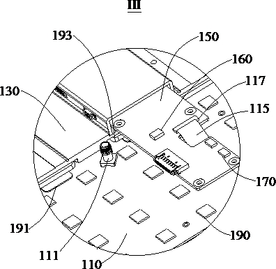
[0035]The flat-panel phased array antenna 100 provided in this embodiment includes a microwave board 110, a structural member 130, a digital circuit board 150, a control unit 160, a power supply unit 170, and multiple antenna radiation units 180. The multiple antenna radiation units 180 are arranged in the microwave On one side surface of the board 110, the structural member 130 is mounted on the other side surface of the microwave board 110, the digital circuit board 150 is mounted on the structural member 130 and is electrically connected to the microwave board 110, and the control unit 160 and the power supply unit 170 are both arranged on On the digital circuit board 150...


PUM


Abstract

An embodiment of the present invention provides a flat-panel phased array antenna, which relates to the field of antenna technology. The flat-panel phased-array antenna includes a microwave board, a structural member, a digital circuit board, a control unit, a power supply unit, and multiple antenna radiation units. An antenna radiating unit is set on one side surface of the microwave board, the structural parts are mounted on the other side surface of the microwave board, the digital circuit board is installed on the structural parts and electrically connected with the microwave board, the control unit and the power supply unit are set on the digital On the circuit board, at least part of the digital circuit board is arranged opposite to the microwave board, and the projection of the digital circuit board on the microwave board is located in the microwave board. Compared with the prior art, the planar phased array antenna provided by the embodiment of the present invention can realize arbitrary splicing and large array formation, and has small size, low processing difficulty and low processing cost.

Description

Technical field[0001]The present invention relates to the technical field of antennas, in particular to a flat-panel phased array antenna.Background technique[0002]In the prior art, in addition to the area of ​​the radiating unit of the flat-panel phased array antenna, usually a part of the area of ​​the antenna array is used for the placement of control and power supply devices and connectors, namely the front radiating unit, control unit, and power supply. Units and connectors are placed on a PCB (printed circuit board), which will cause the following disadvantages:[0003](1) From the perspective of splicing, due to the need to partition the PCB board, some areas are not laid with antenna radiating elements, resulting in the existing array only suitable for 2×n splicing methods, which is not conducive to arbitrary splicing and large array arrays. The reason is that the extra area of ​​the control and power supply unit will cause the antenna to fail to scan normally, and there will ...

Claims


Application Information

Patent Timeline
Patent Type & Authority Patents(China)
IPC IPC(8): H01Q1/36H01Q1/38H01Q1/50H01Q21/00H01Q1/00
CPCH01Q1/02H01Q1/36H01Q1/38H01Q1/50H01Q21/00
Inventor 周锐罗烜路继发崔易彧郭凡玉
Owner CHENGDU T-RAY TECH CO LTD
Why Eureka
Try Eureka