Implementation method of CMOS image sensor

A technology of image sensor and implementation method, applied in the direction of electric solid-state devices, semiconductor devices, electrical components, etc., can solve image retention, photodiode photogenerated electrons cannot be read out, increase photodiode N-type doping dose doping depth, etc. problems, to achieve the effects of reducing readout noise, improving transfer function, and improving electrical performance

Pending Publication Date: 2020-12-29
GALAXYCORE SHANGHAI
View PDF0 Cites 0 Cited by
  • Summary
  • Abstract
  • Description
  • Claims
  • Application Information

AI Technical Summary

Problems solved by technology

[0004] With the shrinking of the feature size of CMOS image sensors, on the one hand, in order to reduce the readout noise of image sensors, high-performance source-follower transistors are required; The N-type dopant dose and doping dept

Method used


Image

  • Implementation method of CMOS image sensor
  • Implementation method of CMOS image sensor
  • Implementation method of CMOS image sensor

Examples


Embodiment Construction

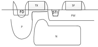
[0044] In the following detailed description of the preferred embodiment, reference is made to the accompanying drawings which form a part hereof. The accompanying drawings show, by way of example, specific embodiments in which the invention can be practiced. The illustrated embodiments are not intended to be exhaustive of all embodiments in accordance with the invention. It is to be understood that other embodiments may be utilized and structural or logical changes may be made without departing from the scope of the present invention. Accordingly, the following detailed description is not limiting, and the scope of the invention is defined by the appended claims.

[0045]It will be apparent to those skilled in the art that the invention is not limited to the details of the above-described exemplary embodiments, but that the invention can be embodied in other specific forms without departing from the spirit or essential characteristics of the invention. Accordingly, the embo...


PUM


Abstract

The invention provides a CMOS (Complementary Metal Oxide Semiconductor) image sensor implementation method. The method comprises the following steps of forming a trench on a semiconductor substrate, and forming a source following transistor of an image sensor pixel unit in the subsequent step by at least part of the trench; filling a third barrier layer to cover the trench; etching a partial region around the trench by adopting a graphical process to form a shallow trench isolation structure; filling an oxide layer to cover the shallow trench isolation structure; chemically and mechanically grinding the oxide layer until reaching the third barrier layer; removing the third barrier layer; and filling the trench with a polycrystalline silicon layer, and etching at least part of the trench toform a source following transistor.

Description

technical field [0001] The invention relates to a method for realizing a CMOS image sensor. Background technique [0002] Image sensors have become ubiquitous. Image sensors are widely used in digital still cameras, cellular phones, surveillance cameras, as well as in medical, automotive and other applications. The technology used to manufacture image sensors continues to advance substantially. For example, demands for higher resolution and lower power consumption have driven further miniaturization and integration of these devices. At present, image sensors can be classified into charge coupled device (CCD, Charge Coupled Device) image sensors and metal oxide semiconductor (CMOS, Complementary Metal-Oxide Semiconductor) image sensors. Among them, due to the high integration, good compatibility, and low power of the CMOS image sensor, and with the improvement of the CMOS manufacturing process, the CMOS image sensor has become the mainstream technology of the current image...

Claims


Application Information

Patent Timeline
IPC IPC(8): H01L27/146
CPCH01L27/14614H01L27/14687H01L27/14689
Inventor 赵立新徐涛
Owner GALAXYCORE SHANGHAI
Why Eureka
Try Eureka