Nitride resonance tunneling diode structure suitable for ultraviolet light detection

A resonant tunneling and nitride technology, which is applied in the direction of electrical components, circuits, semiconductor devices, etc., can solve the problem of resonant tunneling from electrons to double barrier structures, no ultraviolet light detection combination technology, and raising the energy band of GaN intrinsic layer etc. to achieve the effects of low background dark current, enhanced ultraviolet light detection quantum efficiency, and low dark noise

Active Publication Date: 2020-12-29
INST OF ELECTRONICS ENG CHINA ACAD OF ENG PHYSICS
View PDF4 Cites 1 Cited by
  • Summary
  • Abstract
  • Description
  • Claims
  • Application Information

AI Technical Summary

Problems solved by technology

However, the conventional nitride resonant tunneling diode structure is not suitable for the thick intrinsic GaN isolation layer, because the intrinsic built-in polarization electric field of the nitride material will greatly lift the energy bands of the GaN intrinsic layer and the double barrier structure layer. , even making the structure unable to resonate tunneling
figure 1 It is the energy band simulation result of the conventional nitride resonant tunneling diode structure, using a 200nm thick intrinsic GaN layer as the light absorbing layer, it can be seen that whether it is a forward bias vo...

Method used


Image

  • Nitride resonance tunneling diode structure suitable for ultraviolet light detection
  • Nitride resonance tunneling diode structure suitable for ultraviolet light detection
  • Nitride resonance tunneling diode structure suitable for ultraviolet light detection

Examples


Embodiment

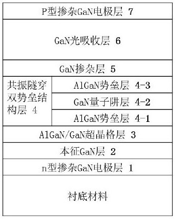
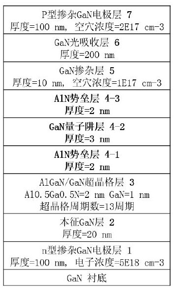
[0030] According to the above-mentioned material structure characteristics, a specific embodiment of the present invention is as follows image 3 shown.

[0031] Using GaN self-supporting substrate material, from the substrate material to the top includes:

[0032] (1) GaN self-supporting substrate material.

[0033] (2) n-type doped GaN electrode layer 1, thickness 100 nm, electron concentration = 5E18 cm -3 .

[0034] (3) Intrinsic GaN layer 2 with a thickness of 20 nm.

[0035] (4) AlGaN / GaN superlattice layer 3, the superlattice is Al0.5Ga0.5N=2 nm, GaN=1 nm periodic structure, and the number of superlattice periods=13 periods.

[0036] (5) Resonant tunneling double barrier structure layer 4, wherein the AlN barrier layer 4-1 has a thickness of 2 nm; the GaN quantum well layer 4-2 has a thickness of 3 nm; the AlN barrier layer 4-3 has a thickness of 2 nm.

[0037] (6) GaN doped layer 5, thickness 10 nm, p-type doped, hole concentration = 1E17 cm -3 .

[0038] (7) Ga...


PUM

PropertyMeasurementUnit
Thicknessaaaaaaaaaa
Thicknessaaaaaaaaaa

Abstract

The invention discloses a nitride resonance tunneling diode structure suitable for ultraviolet light detection, and solves the problems that a conventional nitride resonance tunneling diode structureis not suitable for a thick light absorption layer and cannot perform ultraviolet light detection with high quantum efficiency. According to the invention, a double-barrier resonance tunneling structure is arranged in a p type doped nitride epitaxial layer/intrinsic nitride epitaxial layer/n type doped nitride epitaxial layer, and a built-in polarization electric field of a nitride heterojunctionis counteracted by using the built-in electric field of the p-i-n structure, so that the problem of energy band uplift of the GaN thick light absorption layer is solved, and the nitride resonance tunneling diode structure of the thick light absorption layer can generate resonance tunneling; and an AlGaN/GaN superlattice structure is introduced, and the alignment of a quantum well energy level anda light absorption layer conduction band energy level is adjusted by using the polarization field of the superlattice structure, so that the peak current of resonance tunneling is enhanced.

Description

technical field [0001] The invention belongs to the fields of semiconductor materials and semiconductor photodetectors, and in particular relates to a nitride resonant tunneling diode structure suitable for ultraviolet light detection. Background technique [0002] The resonant tunneling diode is a device based on the resonant tunneling quantum effect. Its basis is a semiconductor heterostructure. Miscellaneous collector) structure. As the external bias voltage of the resonant tunneling diode is gradually increased, the tunneling probability of electrons has a sharp peak at a certain energy value, and the current-voltage curve of the diode also shows a negative differential conductance characteristic. Based on the nonlinear transport characteristics of resonant tunneling diodes, in 2005, J. C. Blakesley et al. proposed a mechanism for local regulation of resonant tunneling current for photon detection [Physical review letters, 2005, 94(6), 067401]. The solution is to use p...

Claims


Application Information

Patent Timeline
IPC IPC(8): H01L31/105H01L31/0304H01L31/0352
CPCH01L31/105H01L31/035236H01L31/03048H01L31/035209
Inventor 王旺平
Owner INST OF ELECTRONICS ENG CHINA ACAD OF ENG PHYSICS
Why Eureka
Try Eureka