Description model and parameter identification method for intrinsic characteristic parameters of MOSFET device

A technology for intrinsic characteristics and description models, which is applied in the field of modeling and parameter identification of intrinsic characteristics of power semiconductor components, and can solve problems such as reducing equation complexity, difficult circuit analysis, and complex circuit system modeling.

Active Publication Date: 2021-01-15
CHINA THREE GORGES UNIV
View PDF8 Cites 4 Cited by
  • Summary
  • Abstract
  • Description
  • Claims
  • Application Information

AI Technical Summary

Problems solved by technology

This method can not only reflect the influence of nonlinear capacitance to a certain extent, but also significantly reduce the complexity of the equation, but it cannot reflect the dynamic characteristics of MOSFET such as the oscillation and Miller platform when turning on and off.
[0007] The third way: use the C-V characteristic curve formula derived from semiconductor physics, reference 6 "Hayati M, Roshani S, Kazimierczuk M K, et al.AClass-E Power Amplifier Design ConsideringMOSFET Nonlinear Drain-to-Source and Nonlinear Gate-to -Drain Capacitances at Any Grading Coefficient[J].IEEE Transactions on Power Electronics,2016,31(11):7770-7779."; Reference 7 "Zhou Lin, Li Hanjiang, Xie Bao, et al. Saber Modeling and Analysis of SiC MOSFET Its application and analysis in photovoltaic grid-connected inverters[J]. Journal of Electrotechnical Society, 2019(20)."; Reference 8 "Liang Mei, Zheng Qionglin, Li Yan, et al. For accurate prediction of SiC MOSFET switching characteristics The analysis model [J]. Acta Electrotechnical Society, 2017, 032 (001): 148-158.") can well realize the change of nonlinear capacitance with bias voltage, and accurately describe the nonlinear characteristics of junction capacitance, but Its physical model is relatively complex, and it is difficult to achieve system-level analysis in complex circuits
[0008] The fourth way: use the function to fit the curve of the nonlinear capacitor changing with the bias voltage, reference 9 "Wu Jianqiang, Li Haoyu. Establishment of the Pspice model of the nonlinear capacitor [J]. Journal of Harbin Institute of Technology, 1999 (03): 44 -46."; Reference 10 "Du Xing, Wang Cuixia, Yu Youling, et al. Matlab circuit simulation model based on SiC MOSFET nonlinear capacitor CGD [J]. Locomotive Electric Transmission, 2020, (01): 49-52. ”), using the behavioral model to model the nonlinear capacitance, the error is small, but in order to describe the change of the junction capacitance with the bias voltage with higher accuracy, a more complex function description is required, which makes the system analysis more complicated. It is not easy to realize system-level circuit analysis
The models in Fig. 2(1) and Fig. 2(2) equate a non-linearly changing capacitance to a time-invariant capacitance and a segmentally varying capacitance, which effectively simplifies the analysis of complex circuit systems; Fig. 2(3 ) Use function fitting to model nonlinear capacitance, multi-parameter or complex functions can accurately reflect the change of capacitance with voltage, and also make the modeling of circuit system complicated

Method used


Image

  • Description model and parameter identification method for intrinsic characteristic parameters of MOSFET device
  • Description model and parameter identification method for intrinsic characteristic parameters of MOSFET device
  • Description model and parameter identification method for intrinsic characteristic parameters of MOSFET device

Examples


Embodiment Construction

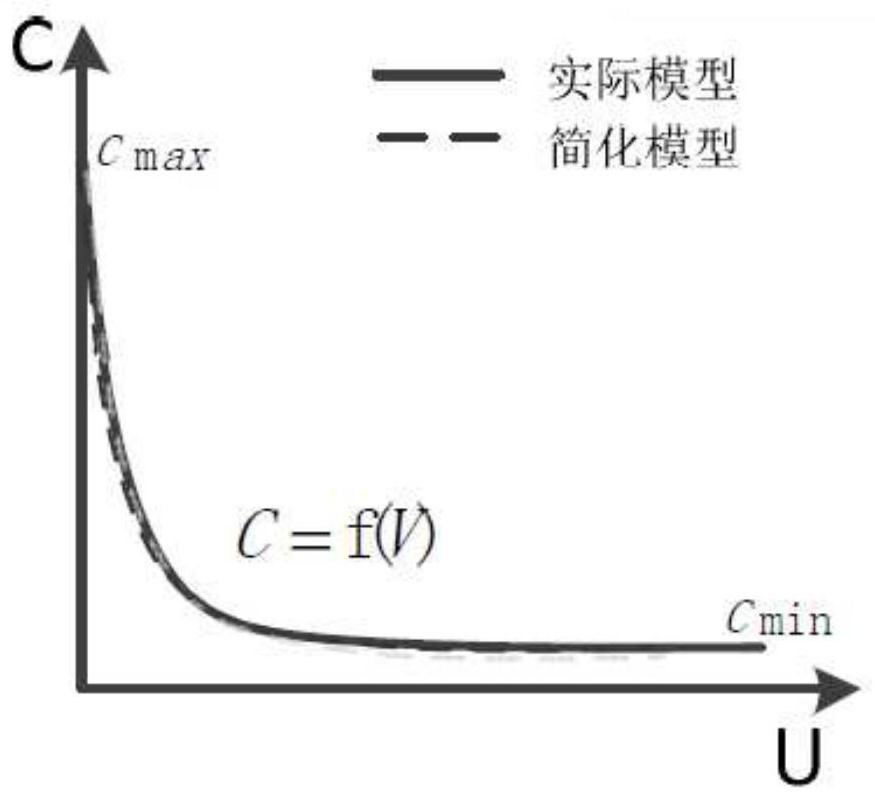
[0059] The present invention will be further described below in conjunction with the N-channel MOSFET whose model is IRF640.

[0060] Such as image 3 , Figure 4 As shown, a description model of the intrinsic characteristic parameters of a MOSFET device is a fractional order model based on the bias voltage of the PN junction capacitance Among them: [K,α] is the parameter to be identified, including:

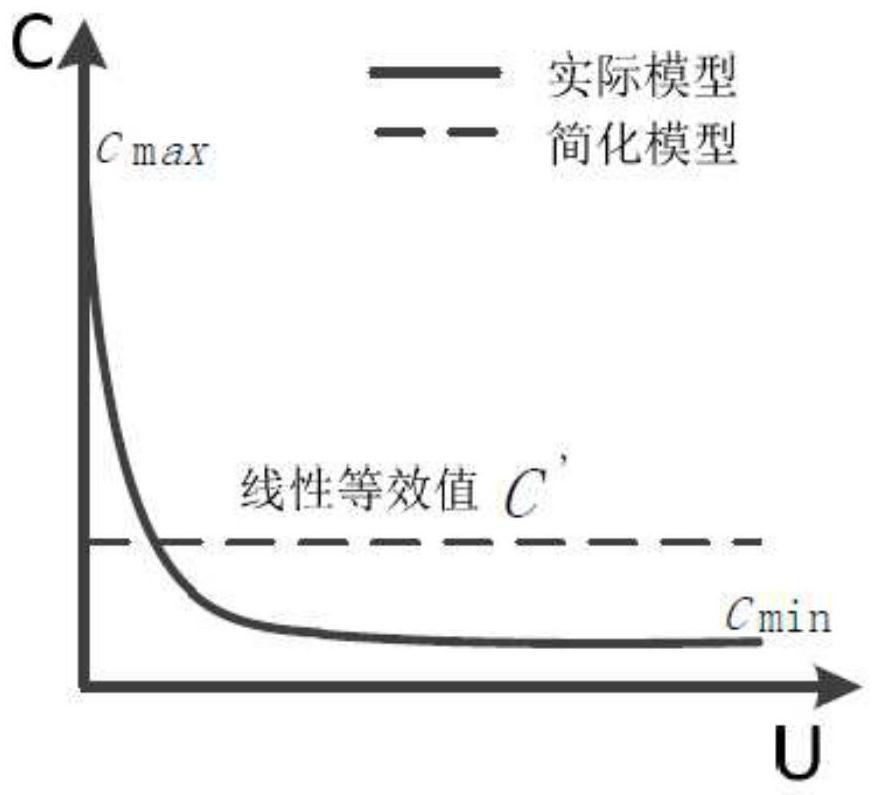
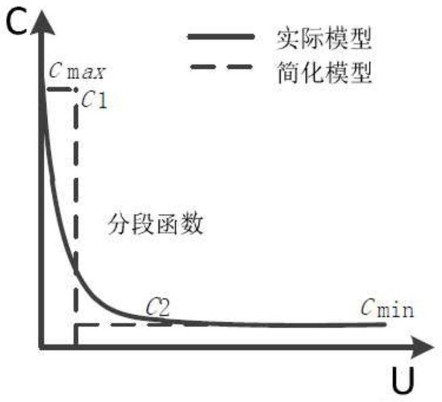
[0061] according to figure 1 , when the MOSFET junction capacitance is in the depletion region under high frequency conditions, the formula for the junction capacitance value is:

[0062]

[0063] where: ε ox is the dielectric constant of the oxide layer, ε s is the dielectric constant of the semiconductor, q is the charge amount of the elementary charge, N A is the doping concentration, d oxide layer thickness, C 0 is the capacitance of the oxide layer, V is the bias voltage;

[0064] For the above formula, usually If the value is larger, formula (1) can be simpli...


PUM


Abstract

The invention relates to a description model and a parameter identification method for intrinsic characteristic parameters of an MOSFET device. The description model is a fractional order model for PNjunction capacitance bias voltage, and the parameter identification method of the description model is a fractional order multi-target offline parameter identification method based on a differentialevolution algorithm. The method comprises the following steps: 1) obtaining data that the capacitance value of the junction capacitor changes along with bias voltage according to a data manual of a certain type of MOSFETs; 2) according to the fractional order model, obtaining the relationship of the junction capacitance with the bias voltage; 3) taking the average absolute percentage error of thefractional order model CE and the corresponding capacitance value in the data manual as a target function of a parameter identification method based on differential evolution to carry out data fitting. The description model provided by the invention can accurately describe the change curve of the intrinsic characteristic parameter PN junction capacitance of the MOSFET device along with the bias voltage, so a reference basis can be provided for the design and reliability analysis of a circuit system containing the element.

Description

technical field [0001] The invention relates to the field of modeling and parameter identification of intrinsic characteristics of power semiconductor components, in particular to a description model and parameter identification method of intrinsic characteristic parameters of a MOSFET device. Background technique [0002] In recent years, the development of power semiconductors is extremely rapid. Among the existing power electronic devices, MOSFET has the characteristics of simple driving, fast switching speed, and relatively cheap production, so it is widely used. After the advent of SiC materials, with the development of process manufacturing level, SiC MOSFET has a higher withstand voltage level, faster turn-on and turn-off speed, and better heat resistance. In the production process of power electronic devices, for example, the parameter characteristics of MOSFET switch tubes are affected by the manufacturing process and working environment, and parameter drift is pron...

Claims


Application Information

Patent Timeline
IPC IPC(8): G06F30/367
CPCG06F30/367Y02B70/10
Inventor 陈曦黄亿席磊
Owner CHINA THREE GORGES UNIV
Why Eureka
Try Eureka