Method and wave absorbing device for realizing broadband light absorption enhancement based on ultrathin metal film

An ultra-thin metal, broadband light technology, used in optics, optical components, instruments, etc., can solve the problems of large overall depth of the device, complex microstructure patterns, etc., and achieve the effect of reducing the depth of the device, good light absorption performance, and reducing costs.

Active Publication Date: 2021-01-22
JIANGNAN UNIV
View PDF18 Cites 9 Cited by
  • Summary
  • Abstract
  • Description
  • Claims
  • Application Information

AI Technical Summary

Problems solved by technology

[0006] The invention provides a method and absorbing device for realizing broadband light absorption enhancement based on an ultra-thin metal film, which solves at least one of the following technical problems: the broadband light absorption enhancement device realized by the current method often relies on relatively complex microstructure patterns , or a larger number of "metal-dielectric" film stacks, the overall depth of the device is larger, and a thicker metal film layer is required

Method used


Image

  • Method and wave absorbing device for realizing broadband light absorption enhancement based on ultrathin metal film
  • Method and wave absorbing device for realizing broadband light absorption enhancement based on ultrathin metal film
  • Method and wave absorbing device for realizing broadband light absorption enhancement based on ultrathin metal film

Examples


Embodiment 1

[0047] Example 1: A wave-absorbing device based on ultra-thin metal film to realize enhanced broadband light absorption

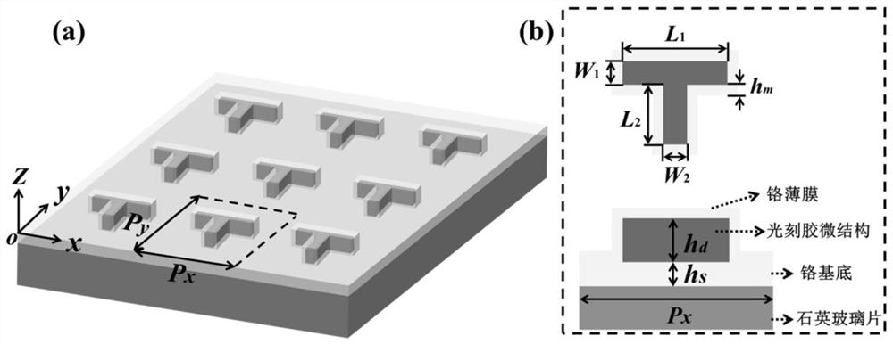
[0048] The broadband light absorption device is realized based on the microstructure of ultra-thin metal film, and its structure and its cells are as follows figure 1 (a)-(b) shown. The structure is placed on a quartz glass sheet. Since the structure is a periodic structure, for a unit cell, from bottom to top, there are chromium substrate, T-shaped photoresist microstructure array, and ultra-thin chromium wrapped T-shaped photoresist microstructure. film layer, period of microstructure P x =P y =P (P is the period of the array along the x and y directions). (b) is a schematic diagram of the cell structure, where the thickness of the chromium substrate is h s , the depth of the T-type photoresist microstructure is h d , the thickness of the chromium film covering the outside is h m ; The length and width of the horizontal bar (x direction bar) of the ...

Embodiment 2

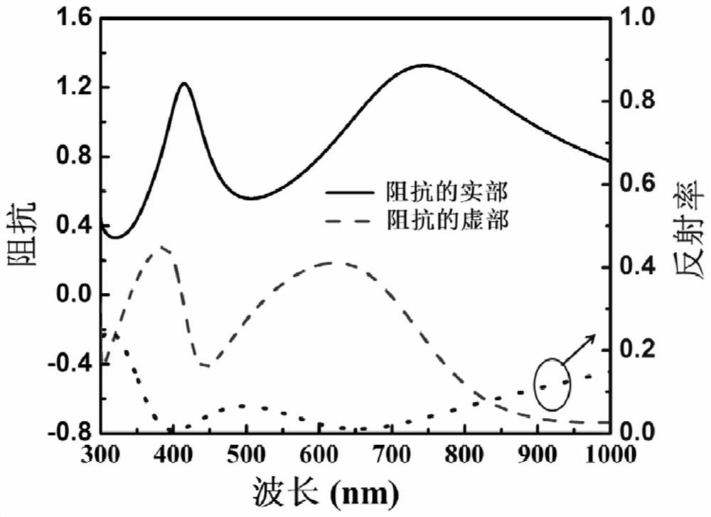
[0064] Example 2: Method for Evaluating Broadband Light Absorption Performance Based on Microstructure Adjustment Impedance

[0065] This embodiment adopts a sub-wavelength structure, and the change of the surface parameters of the microstructure will change the impedance of the structure. Based on the surface plasmon resonance effect of the metal microstructure, when adjusting and optimizing the size and depth of the microstructure to achieve impedance matching , can achieve good broadband light absorption effect. The adjustment range of the microstructure size in the actual design is: the period of the microstructure is smaller than the wavelength of the incident light (visible light band is less than 400nm), and the length and width of the microstructure are smaller than its period; the depth of the microstructure is also smaller than the incident light wavelength (visible light band is less than 400nm). less than 400nm). Use FDTD or FEM method within the above range to ca...

Embodiment 3

[0072] Example 3: A method for realizing broadband microwave absorption with high fabrication tolerance based on ultra-thin metal film

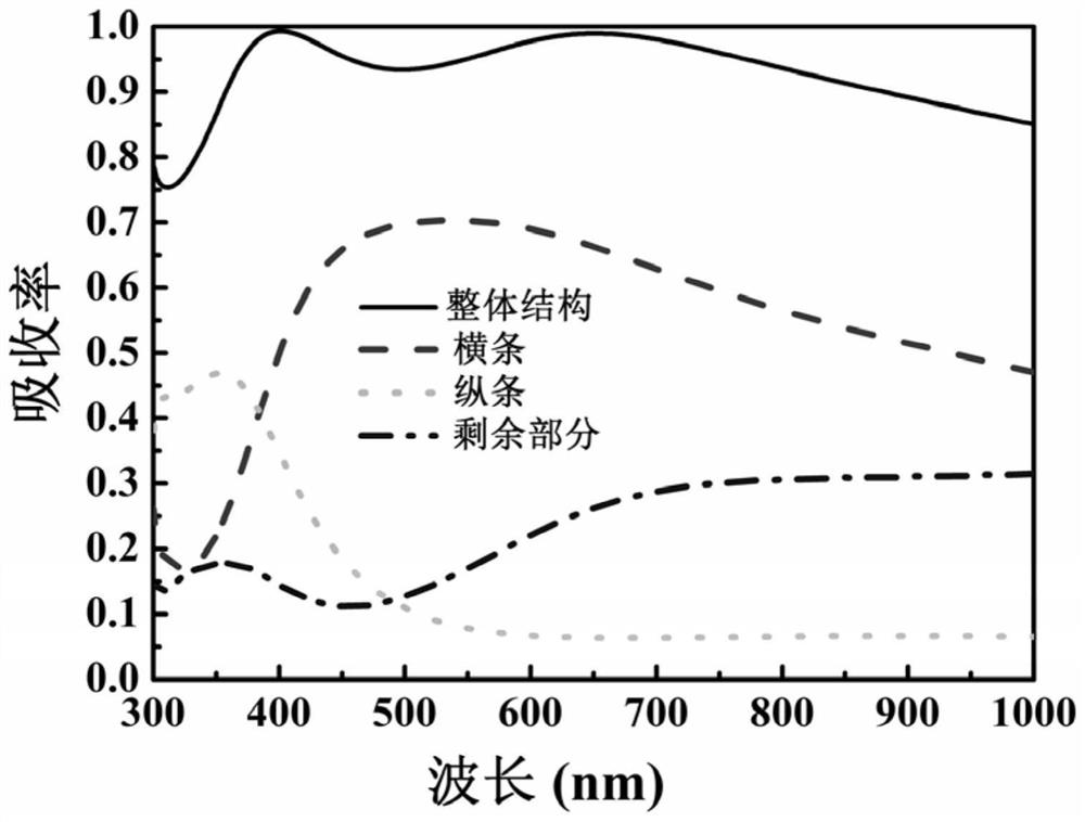
[0073] Since the electric fields of light waves of different wavelengths are localized and enhanced on the surface of different parts of the metal microstructure array, the broadband absorption performance of the structure is manifested as the cooperative absorption effect of different parts in the structure, so the structure presents a very high fabrication tolerance.

[0074] Exploring the thickness h of the chromium film layer in the structure m , the depth h of the photoresist microstructure d , the period P of the microstructure, the influence of the symmetry parameter ΔX of the microstructure on the absorption spectrum, and other structural parameters are the same as in Example 1. From Figure 4 It can be seen in (a) that when the photoresist microstructure is not wrapped by the ultrathin chromium film (h m =0), since the surface pla...


PUM

PropertyMeasurementUnit
thicknessaaaaaaaaaa
thicknessaaaaaaaaaa
thicknessaaaaaaaaaa

Abstract

The invention discloses a method and a wave absorbing device for realizing broadband light absorption enhancement based on an ultrathin metal film, and belongs to the field of micro-nano optics and metamaterial. The structure of the device is sequentially composed of a metal substrate, a T-shaped photoresist microstructure and an ultrathin metal film layer wrapping the T-shaped photoresist microstructure. When incident light irradiates the surface of the device, by means of the surface plasmon resonance effect excited by the metal microstructure array, optical wave electric fields with different wavelengths are highly localized and enhanced on the surfaces of different parts of the T-shaped metal microstructure array, and the size and depth of the T-shaped microstructure are adjusted and optimized to achieve impedance matching. and broadband light absorption enhancement can be realized in the whole visible light band. Besides, the method and the device provided by the invention have very high structure preparation tolerance, are insensitive to incident light polarization state and incident angle change, are beneficial to low-cost preparation, and have extremely high application value in the fields of photoelectric detection, photo-thermal conversion, solar cells, photoelectric imaging, optical stealth and the like.

Description

technical field [0001] The invention relates to a method and a wave-absorbing device for realizing broadband light absorption enhancement based on an ultra-thin metal film, and belongs to the field of micro-nano optics and metamaterials. Background technique [0002] The interaction of light and matter is an issue of great interest in fundamental research and technological applications. Generally, in order to enhance the interaction between light and matter, it is often necessary to improve the response of materials or devices to light, and the enhancement of light absorption in a specific wavelength band is one way to achieve it. Since the enhancement of light absorption is often accompanied by a high degree of localization of the energy of the light field, and causes a significant increase in the electromagnetic field, it can effectively enhance the interaction between light and matter, so in photoelectric detection, photothermal conversion, solar cells, fluorescence spect...

Claims


Application Information

Patent Timeline
Patent Type & Authority Applications(China)
IPC IPC(8): G02B5/00
CPCG02B5/003G02B5/008
Inventor 桑田王勋李国庆裴姚米晴
Owner JIANGNAN UNIV
Why Eureka
Try Eureka