Control method of plasma dry etching process

A plasma and dry etching technology, which is applied in semiconductor/solid-state device manufacturing, electrical components, circuits, etc., can solve the problems affecting the production capacity of the machine and increase the cost, so as to reduce the process cost, improve the production capacity of the machine, and accurately and the effect of stabilizing the control

Active Publication Date: 2021-01-22
SHANGHAI HUALI INTEGRATED CIRCUTE MFG CO LTD
View PDF8 Cites 0 Cited by
  • Summary
  • Abstract
  • Description
  • Claims
  • Application Information

AI Technical Summary

Problems solved by technology

This not only increases the cost, but also affects the production capacity of the machine

Method used


Image

  • Control method of plasma dry etching process
  • Control method of plasma dry etching process
  • Control method of plasma dry etching process

Examples


Embodiment Construction

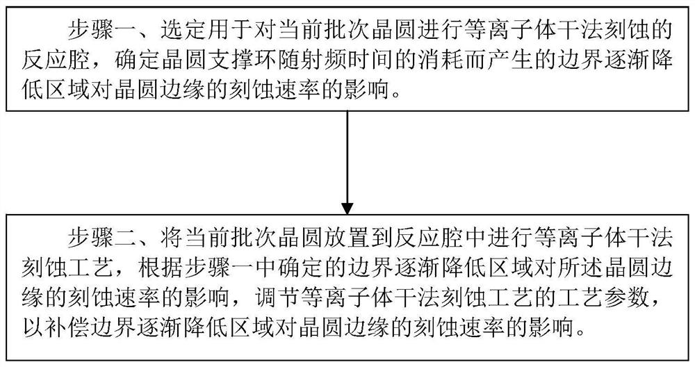
[0033] The method of the embodiment of the present invention is obtained on the basis of analyzing the technical problems existing in the existing method. Before introducing the technical solution of the method of the embodiment of the present invention in detail, the existing technical problems are described as follows:

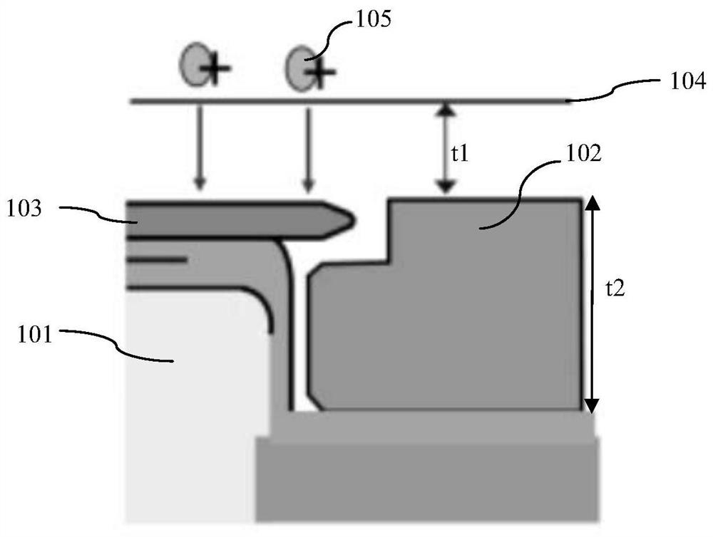
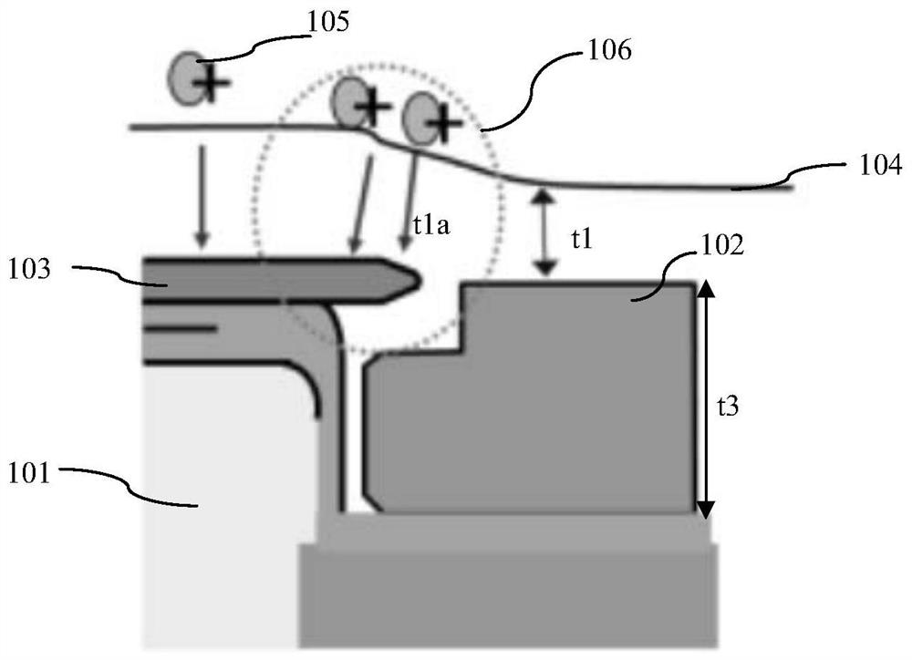
[0034] Such as Figure 1A Shown is a schematic diagram of the structure of the plasma sheath boundary when the wafer support ring is just replaced in the reaction chamber of the plasma dry etching process; the reaction chamber includes a wafer placement area 101 and a wafer placement area 101. The wafer support ring 102 on the peripheral side, the wafer 103 is placed on the wafer placement area 101, and the wafer placement area 101 is provided with an electrostatic adsorption plate, and the wafer 103 is fixed by the electrostatic adsorption plate.

[0035] The reaction chamber also includes a radio frequency source. After the process gas is introduced, a plas...


PUM


Abstract

The invention discloses a method for controlling a plasma dry etching process, and the method comprises the following steps: 1, selecting a reaction cavity for performing plasma dry etching on a current batch of wafers, and determining the influence of a boundary gradually-reduced region generated by a wafer support ring along with the consumption of radio frequency time on the etching rate of theedge of the wafer; 2, placing the current batch of wafers into a reaction chamber to carry out a plasma dry etching process, and adjusting process parameters of the plasma dry etching process according to the influence of the boundary gradually-reduced area determined in the step 1 on the etching rate of the wafer edge, so that the influence of the area on the etching rate of the wafer edge is gradually reduced by the compensation boundary. The wafer edge etching depth can be kept stable, the service life of parts of the reaction cavity can be prolonged, and the process time between two timesof cavity opening can be prolonged, so the process cost is reduced, and the productivity of a machine table is improved.

Description

technical field [0001] The invention relates to a method for manufacturing a semiconductor integrated circuit, in particular to a method for controlling a plasma dry etching process. Background technique [0002] With the continuous shrinking of the critical dimensions of integrated circuits and the continuous improvement of the integration of microelectronic devices, advanced plasma etching processes have been introduced into the wafer manufacturing process. [0003] During the plasma etching process, the reactive gas is dissociated under the excitation of radio frequency current to generate active plasma. On the one hand, the plasma reacts with the part of the wafer not covered by the photoresist to transfer the circuit pattern to the wafer; on the other hand, the plasma reacts with the components of the reaction chamber, which makes the components continue to be consumed with the increase of radio frequency time , resulting in a change in the cavity plasma distribution. ...

Claims


Application Information

Patent Timeline
Patent Type & Authority Applications(China)
IPC IPC(8): H01L21/3065
CPCH01L21/3065Y02P90/02
Inventor 李光磊林永顺吴庆仁
Owner SHANGHAI HUALI INTEGRATED CIRCUTE MFG CO LTD
Why Eureka
Try Eureka