P-type crystalline silicon solar cell with tunneling passivation and preparation method thereof

A technology of solar cells and crystalline silicon, applied in circuits, photovoltaic power generation, electrical components, etc.

Pending Publication Date: 2021-02-02
TRINA SOLAR CO LTD +1
View PDF0 Cites 6 Cited by
  • Summary
  • Abstract
  • Description
  • Claims
  • Application Information

AI Technical Summary

Problems solved by technology

In recent years, the progress of domestic crystalline silicon solar cell technology is still mainly focused on the industrial introduction of PERC cells. Although the production capacity of P-type PERC cells has been increasing, the growth of its industrialization efficiency may be close to saturation. Therefore, it is urgent to develop the next For the first generation of PERC cells, it is hoped that on the basis of the original production line, the process changes can be minimized to achieve a breakthrough in product performance and cost

Method used


Image

  • P-type crystalline silicon solar cell with tunneling passivation and preparation method thereof

Examples


Embodiment 1

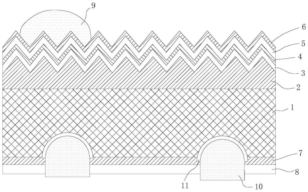
[0036] like figure 1 As shown, this embodiment provides a P-type crystalline silicon solar cell with tunneling passivation, including a P-type substrate 1, characterized in that the front of the P-type substrate 1 is sequentially provided with Selective emitter 2, ultra-thin tunneling silicon oxide layer 3, phosphorus-doped polysilicon layer 4, front silicon oxide passivation layer 5 and front silicon nitride passivation layer 6, the back of the P-type substrate 1 is composed of inner To the outside, the back aluminum oxide passivation layer 7 and the back silicon nitride siliconization layer 8 are sequentially arranged, the front silicon nitride passivation layer 6 is provided with a front metal silver grid line 9, and the back side of the P-type substrate 1 is provided with a back metal aluminum grid line 10 , the back metal aluminum grid line 10 runs through the back aluminum oxide passivation layer 7 and the back silicon nitride silicide layer 8 , and there is a back local...

Embodiment 2

[0040] like figure 1 Shown, a kind of preparation method of the p-type crystalline silicon solar cell with tunneling passivation comprises the following steps:

[0041] 1) Phosphorus diffusion is carried out on the front side of the silicon wafer after texturing. The phosphorus diffusion uses low pressure or normal pressure diffusion, and the square resistance is between 100ohm / sq-300ohm / sq.

[0042] 2) The front side is heavily doped with laser PSG to form a selective emitter layer. The difference between the rear resistance of laser PSG heavy doping and the original square resistance is between 30ohm / sq-150ohm / sq,

[0043] 3) After removing the PSG, an ultra-thin tunneling silicon oxide layer 3 and an amorphous silicon layer are sequentially prepared on the front side of the silicon wafer. The amorphous silicon layer is an in-situ phosphorus-doped amorphous silicon film or an intrinsic amorphous silicon film. When the amorphous silicon layer is an intrinsic amorphous silico...

Embodiment 3

[0055] A method for preparing a p-type crystalline silicon solar cell with tunneling passivation, specifically as follows:

[0056] P-type single crystal silicon is used as a substrate, and conventional texturing is carried out in a solution containing KOH and texturing additives. After cleaning with hydrofluoric acid and RCA, phosphorus is diffused on the front side of the silicon wafer, and the square resistance is about 150ohm / sq. The front side of the silicon wafer is heavily doped with conventional laser PSG, and the square resistance is 65-75ohm / sq. Because the thickness of amorphous silicon is very thin, the slurry is easy to burn through when the screen is sintered, so the emitter is in contact with the laser PSG heavily doped, that is, the front side is actually a selective emitter, and it has better opening pressure and touch. After cleaning with hydrofluoric acid and RCA, prepare a layer of ultra-thin tunneling silicon oxide with a thickness of 1nm-3nm on the fron...


PUM

PropertyMeasurementUnit
thicknessaaaaaaaaaa
thicknessaaaaaaaaaa
thicknessaaaaaaaaaa

Abstract

The invention belongs to the technical field of crystalline silicon solar cells, and relates to a P-type crystalline silicon solar cell with tunneling passivation and a preparation method thereof. Thesolar cell comprises a P-type substrate, and is characterized in that a selective emitter, an ultrathin tunneling silicon oxide layer, a phosphorus-doped polycrystalline silicon layer, a front silicon oxide passivation layer and a front silicon nitride passivation layer are sequentially arranged on the front face of the P-type substrate from inside to outside, and a back aluminum oxide passivation layer and a back silicon nitride silicification layer are sequentially arranged on the back face of the P-type substrate from inside to outside; A front metal silver grid line is arranged on the front silicon nitride passivation layer, a back metal aluminum grid line is arranged on the back face of the P-type substrate, and the back metal aluminum grid line penetrates through the back aluminum oxide passivation layer and the back silicon nitride silicification layer. The structure is very thin, the problem of light absorption of the silicon wafer is solved, the surface recombination rate ofthe cell is effectively reduced, the front passivation of the cell is improved, and the performance of the cell is improved.

Description

technical field [0001] The invention belongs to the technical field of crystalline silicon solar cells, and relates to a patterned passivation contact solar cell and a manufacturing method thereof. Background technique [0002] In recent years, photovoltaic industrialization technology has developed rapidly, and all manufacturing links have technological updates. New technologies and new processes bring lower costs and better product performance. In recent years, the progress of domestic crystalline silicon solar cell technology is still mainly focused on the industrial introduction of PERC cells. Although the production capacity of P-type PERC cells has been increasing, the growth of its industrialization efficiency may be close to saturation. Therefore, it is urgent to develop the next For the first-generation PERC battery, it is hoped that on the basis of the original production line, process changes can be minimized to achieve breakthroughs in product performance and co...

Claims


Application Information

Patent Timeline
Patent Type & Authority Applications(China)
IPC IPC(8): H01L31/0216H01L31/068H01L31/18
CPCH01L31/02167H01L31/0682H01L31/1804H01L31/1864H01L31/1868Y02E10/546Y02E10/547Y02P70/50
Inventor 陈姝冯志强
Owner TRINA SOLAR CO LTD
Why Eureka
Try Eureka