
Organic compounds, polymers, mixtures, compositions and electronic devices

A technology for organic compounds and electronic devices, applied in the fields of polymers, mixtures, organic compounds, compositions and electronic devices, can solve the problem of little research on thermally activated delayed fluorescent materials, improve exciton utilization, reduce energy Loss, inhibition of coupling effect

Active Publication Date: 2022-05-17
GUANGDONG JUHUA PRINTING DISPLAY TECH CO LTD
View PDF13 Cites 0 Cited by
  • Summary
  • Abstract
  • Description
  • Claims
  • Application Information

AI Technical Summary

Problems solved by technology

[0004] In recent years, thermally activated delayed fluorescent materials have been a popular direction, and thermally activated delayed fluorescent materials can also be used as host materials to improve device performance, especially for phosphorescent materials, which can improve device efficiency and life as host materials. It is obvious; however, people pay more attention to the characteristics that it can use singlet and triplet excitons simultaneously as a luminescent material, and there are few studies on thermally activated delayed fluorescent materials used as host materials

Method used


Image

  • Organic compounds, polymers, mixtures, compositions and electronic devices
  • Organic compounds, polymers, mixtures, compositions and electronic devices
  • Organic compounds, polymers, mixtures, compositions and electronic devices

Examples


preparation example Construction

[0138] According to the above-mentioned preparation method, the above-mentioned formed functional layer has a thickness of 5nm-1000nm.

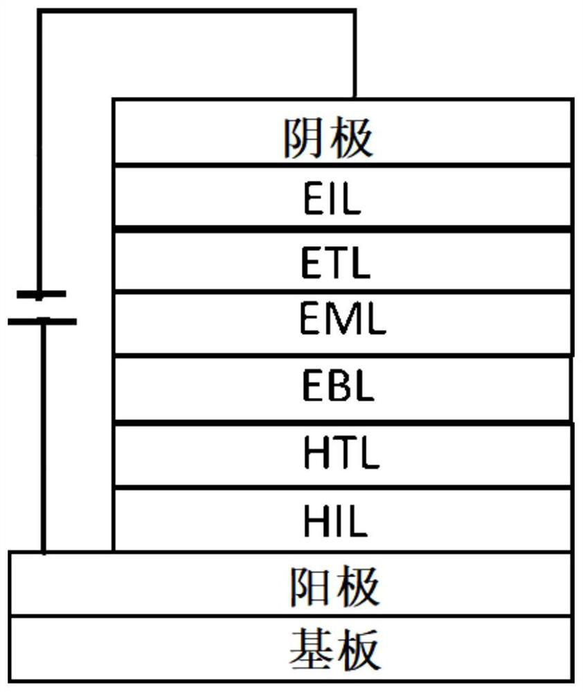
[0139] Furthermore, an embodiment of the present invention also provides an electronic device, which includes: a functional layer, and the material forming the functional layer includes at least one of the above-mentioned organic compound, the above-mentioned high polymer or the above-mentioned mixture kind.

[0140] In a preferred embodiment, the forming material of at least one functional layer in the electronic device includes at least one of the above-mentioned organic compound or the above-mentioned high polymer or the above-mentioned mixture, and wherein at least one of the above-mentioned organic compound Or the above-mentioned high polymer or the above-mentioned mixture is used as the host material.

[0141] Further, the above-mentioned functional layers are optional but not limited to: such as hole injection layer (HIL (, hole trans...

specific Embodiment

[0152] Here are examples of organic compounds, electronic device-based preparation methods and applications according to the present invention, but the present invention is not limited to the following examples.

[0153] An embodiment of the present invention provides a preparation method for synthesizing the organic compound of the present invention, comprising the steps of:

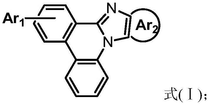
[0154] Under a nitrogen atmosphere, in an organic solvent, the compound represented by the general formula M-1 reacts with the compound represented by the general formula M-2 or M-3 under the action of a catalyst to obtain the organic compound of the present invention.

[0155]

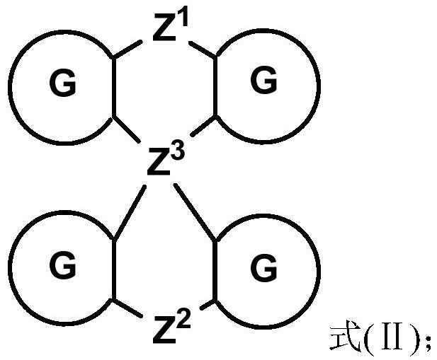
[0156] Among them, Ar 2 ,Z 1 ,Z 2 ,Z 3 , The implication of G is the same as claim 1.

[0157] Taking compound T1-T22 as an example, general formula M-1 is selected from compound (1-1( or (1-2(.

[0158]

[0159] General formula M-2 is selected from compound formula (2-1(-(2-7() in any one.

[0160]

[0161] Gene...

Embodiment 1

[0165] Synthetic compound T1, concrete steps are as follows:

[0166] Add 3.6mmol compound (1-1(, 3.0mmol compound (3-1(, 3.6mmol sodium tert-butoxide, 0.1mmol palladium acetate Pd(OAc( 2 , 0.3mmol tri-tert-butylphosphine tetrafluoroborate [( t Bu( 3 PH]BF 4 , and then repeated 3 times of vacuum pumping and nitrogen exchange, adding 50mL of toluene, and reflux reaction at 110°C for 24h under nitrogen atmosphere. After the reaction was completed, the suspension was cooled to room temperature, poured into water, extracted 3 times with dichloromethane, and then washed with anhydrous MgSO 4 The extract was dried, filtered, and the solvent was removed by rotary evaporation to obtain a crude product. The crude product was separated and purified by silica gel chromatography, using n-hexane / dichloromethane as eluent, rotary evaporation, and drying to remove the solvent to obtain compound T1. The reaction process is as follows:

[0167]

[0168] The molecular formula of compoun...


PUM

PropertyMeasurementUnit
thicknessaaaaaaaaaa
glass transition temperatureaaaaaaaaaa

Abstract

The invention relates to an organic compound, a high polymer, a mixture, a composition and an electronic device. The organic compound is represented by formula (I), and the organic compound is a thermally activated delayed fluorescent material with a wide energy gap. The organic compound and Compositions and mixtures containing the organic compound have great potential applications in the fields of electroluminescence, photovoltaic cells, sensors and the like, and the prepared electronic devices have high efficiency and long service life.

Description

technical field [0001] The invention relates to the field of organic luminescent materials, in particular to an organic compound, a high polymer, a mixture, a composition and an electronic device. Background technique [0002] Organic light-emitting diode (OLEDs) displays are gradually becoming the mainstream of high-end displays, such as high-end flagship mobile phones, high-end TVs, fashion lighting, VR / AR wearable displays, etc. Nevertheless, OLED still has its disadvantages, such as screen burn-in and color shift, which are widely concerned. This is caused by the difference in luminous life of red, green and blue devices. Burn-in, color cast and other issues. [0003] The lifespan of OLED devices is closely related to the device structure and materials. Optimizing the device structure of a specific material is very limited in improving the lifespan. Starting from the improvement of material research and development, there is still a lot of room for improvement in device...

Claims


Application Information

Patent Timeline
Patent Type & Authority Patents(China)
IPC IPC(8): C07D471/04C07F7/10C07D519/00C09K11/06H01L51/50H01L51/54
CPCC07D471/04C07F7/0816C07D519/00C09K11/06C09K2211/1007C09K2211/1029C09K2211/1033C09K2211/1044C09K2211/1088C09K2211/104H10K85/111H10K85/6574H10K85/657H10K85/6572H10K50/00Y02E10/549
Inventor 周兴邦
Owner GUANGDONG JUHUA PRINTING DISPLAY TECH CO LTD
Learn More