Semiconductor structure and manufacturing method thereof

A manufacturing method and semiconductor technology, applied in semiconductor/solid-state device manufacturing, gaseous chemical plating, coating, etc., to achieve the effect of improving isolation effect, improving production efficiency, and good compactness

Pending Publication Date: 2021-02-09
CHANGXIN MEMORY TECH INC
View PDF4 Cites 0 Cited by
  • Summary
  • Abstract
  • Description
  • Claims
  • Application Information

AI Technical Summary

Problems solved by technology

However, the existing shallow trench isolation s

Method used


Image

  • Semiconductor structure and manufacturing method thereof
  • Semiconductor structure and manufacturing method thereof
  • Semiconductor structure and manufacturing method thereof

Examples


Embodiment Construction

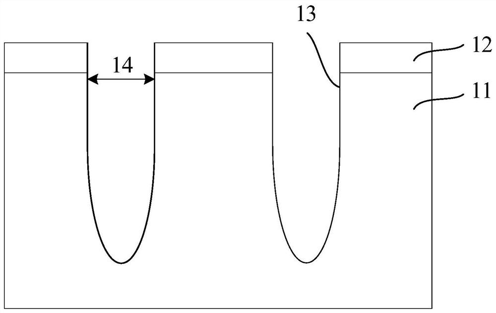
[0028] The manufacturing process of the semiconductor structure includes: after etching a trench with a preset depth and width in the substrate, filling the trench with an insulating substance. Ideally, the insulating substance has good adhesion to the sidewall and bottom of the trench, and the insulating substance attached to the sidewall and bottom of the trench has good compactness, ensuring that ions in the substrate will not diffuse through the isolation structure to adjacent cells, affecting the electrical performance and product yield of the semiconductor structure.

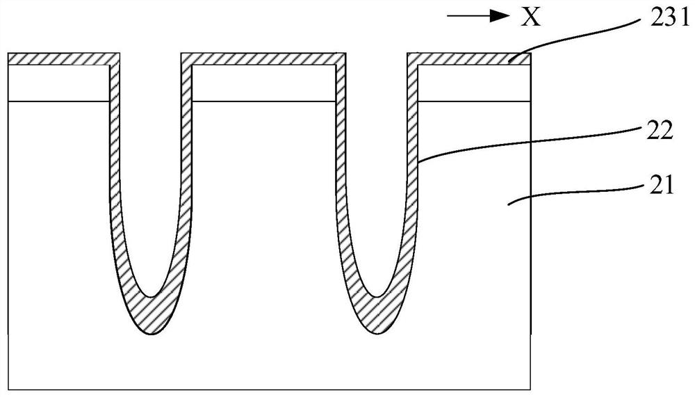
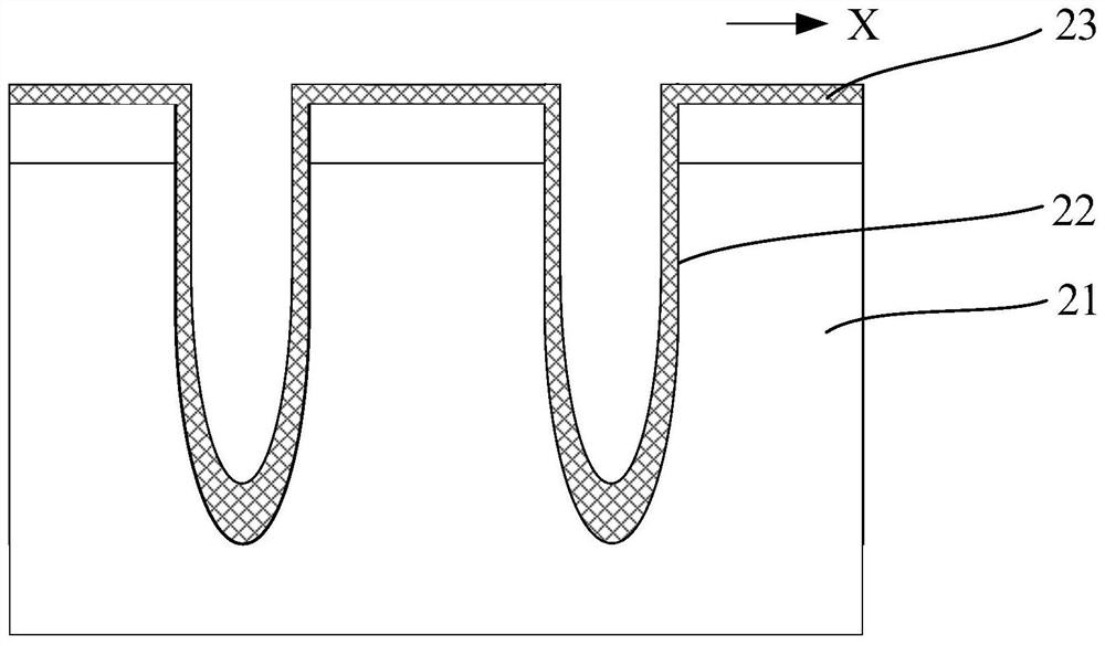
[0029] At present, the main method of manufacturing semiconductor structures is: after etching a trench with a predetermined depth and opening width in the substrate, the plasma enhanced atomic layer deposition (Plasma Enhanced Atomic Layer Deposition, PEALD) is used to fill the trench. insulating substance until the trench opening is closed.

[0030] However, the plasma-enhanced atomic layer deposition p...


PUM


Abstract

The embodiment of the invention relates to a semiconductor structure and a manufacturing method thereof, and the manufacturing method of the semiconductor structure comprises the steps: providing a substrate which is internally provided with a trench; forming a first isolation layer on the side walls and the bottom of the trench by adopting thermal atomic layer deposition; and forming a second isolation layer on the surface of the first isolation layer, and filling the trench with the second isolation layer, wherein the process of forming the second isolation layer comprises at least one plasma enhanced atomic layer deposition process. The method is beneficial to reducing the leakage current of the semiconductor structure and improving the electrical performance and yield of the semiconductor structure.

Description

technical field [0001] The invention relates to the technical field of semiconductors, in particular to a semiconductor structure and a manufacturing method thereof. Background technique [0002] With the advancement of semiconductor manufacturing technology and the continuous improvement of people's demand for the convenience of electronic devices, semiconductor structures are widely used in digital circuits and analog circuits, and the high integration and miniaturization of circuits has become the current development trend. As the size of semiconductor devices shrinks, isolation structures in the devices become more and more important. . [0003] At present, the shallow trench isolation technology is used to replace the traditional intrinsic oxidation isolation technology, and the purpose of isolation is achieved by forming a shallow trench and then filling the trench with an insulating material. The insulating substance is mainly a combination of silicon dioxide and si...

Claims


Application Information

Patent Timeline
IPC IPC(8): H01L21/762C23C16/513C23C16/455
CPCH01L21/76232C23C16/45525C23C16/513
Inventor 黄其赞
Owner CHANGXIN MEMORY TECH INC
Why Eureka
Try Eureka