

Wafer anti-sticking device
An anti-sticking, wafer technology, applied in electrical components, semiconductor/solid-state device manufacturing, circuits, etc., can solve problems such as shadow effect, clamp ring wafer sticking, etc.
- Summary
- Abstract
- Description
- Claims
- Application Information
AI Technical Summary
Problems solved by technology
Method used
Image

Examples
Embodiment
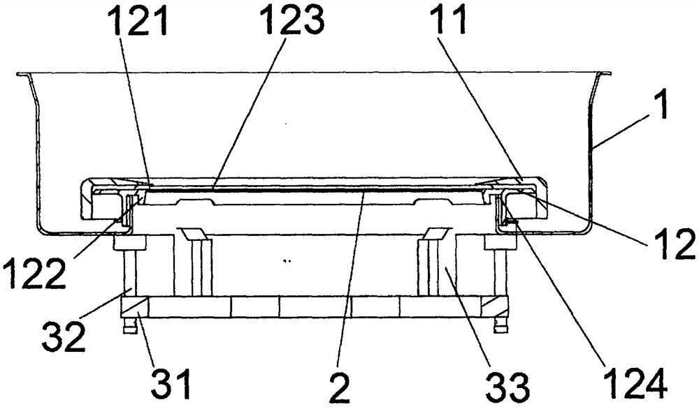
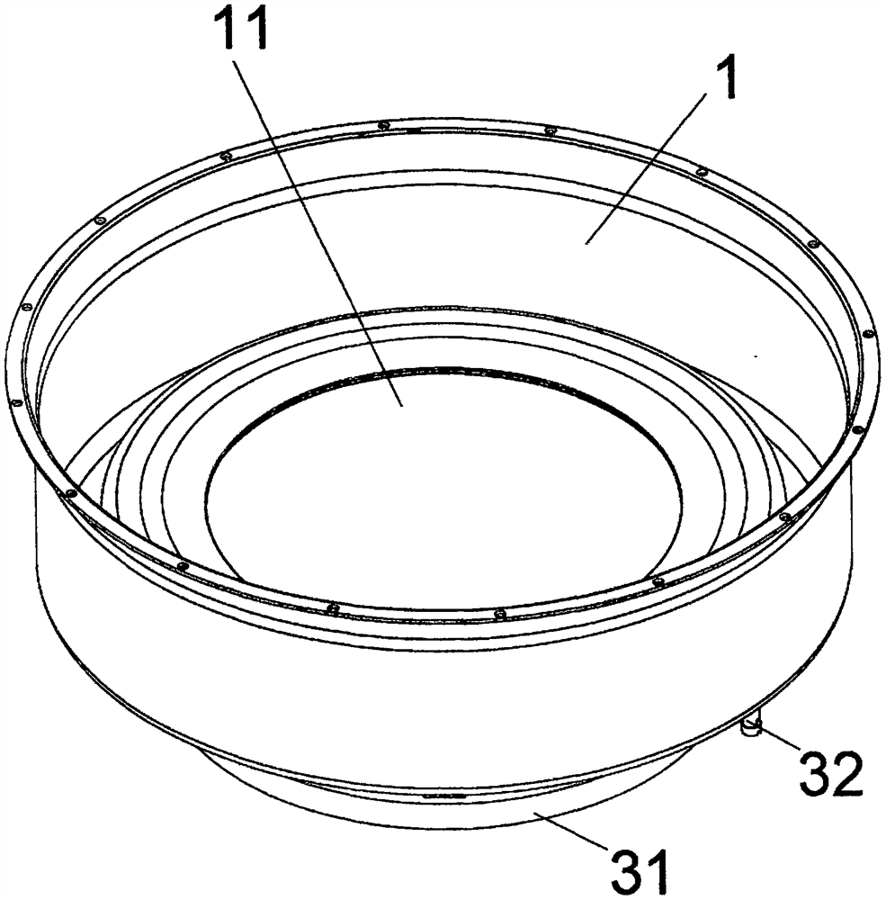
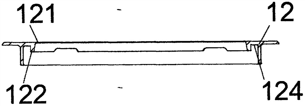
[0017] see Figure 1-4 As shown, the present invention provides a technical solution for a wafer anti-sticking device: it includes a protective cover 1, the bottom wall of the protective cover 1 is arranged in a through shape, the bottom of the protective cover 1 is provided with a lifting assembly, and a top shield is provided above the lifting assembly. Plate 11, specifically, the top shielding plate 11 is used to provide a shielding function for the lower clamping ring, and to prevent deposition at the wafer clamping contact point 121 between the lower edge clamping ring 122 and the edge of the wafer 2 during the deposition process, the top The shielding plate 11 is adapted to the bottom of the protective cover 1, and the top inner wall of the top shielding plate 11 is provided with a lower clamping ring 12, and the upper inner wall of the lower clamping ring 12 is provided with a wafer clamping contact point 121, and the wafer clamping contacts The point 121 is used to cla...
PUM
 Abstract
Description
Claims
Application Information