Multi-layer microstrip board processing method based on perovskite ceramic filling substrate

A processing method and perovskite technology are applied in multilayer circuit manufacturing, circuit metal processing, and electrical connection formation of printed components, etc., which can solve the problems of difficult deposition of copper layers, poor adhesion and easy falling off, poor hydrophilicity, etc., and achieve High surface activity, less microscopic defects, and improved adhesion

Active Publication Date: 2021-02-19
CHINA ELECTRONIC TECH GRP CORP NO 38 RES INST
View PDF5 Cites 2 Cited by
  • Summary
  • Abstract
  • Description
  • Claims
  • Application Information

AI Technical Summary

Problems solved by technology

[0007] The technical problem to be solved by the present invention is: how to solve the problem of many edge burrs, poor hydrophilicity, difficult deposition of copper layer, easy cavity and cracking of copper plating layer, poor adhesion and easy falling off after deposition in the traditional multilayer microstrip board processing. To solve the problems of low reliability, a multilayer microstrip plate processing method based on perovskite ceramic filled substrate is provided

Method used


Image

  • Multi-layer microstrip board processing method based on perovskite ceramic filling substrate
  • Multi-layer microstrip board processing method based on perovskite ceramic filling substrate
  • Multi-layer microstrip board processing method based on perovskite ceramic filling substrate

Examples


Embodiment 1

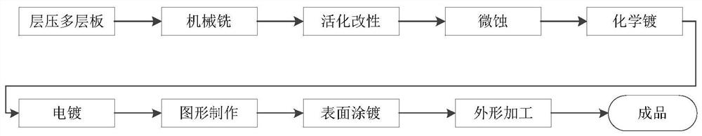
[0040] Such as figure 1 As shown, the present embodiment provides a technical solution: a method for processing a multilayer microstrip plate based on a perovskite ceramic filled substrate, comprising the following steps:

[0041] (1) A multi-layer board based on perovskite ceramic filled microwave dielectric board is obtained by lamination, and the inner wall of the blind slot or the side wall of the through slot is obtained by mechanical milling;

[0042] (2) Activate and modify the inner wall of the blind groove or the side wall of the shape of the through groove;

[0043] (3) Micro-etch the inner wall of the blind groove or the side wall of the through groove; improve the adhesion of the copper plating;

[0044] (4) Electroless copper plating is performed on the inner wall of the blind slot or the side wall of the through slot;

[0045] (5) Electroplating copper is thickened on electroless copper plating;

[0046] (6) Carry out surface coating together with the whole pl...

Embodiment 2

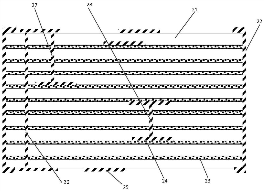
[0072] Such as figure 2 Shown is a schematic diagram of metallization on the side of the shape in this embodiment. The semi-finished 20-layer microstrip board after lamination includes: 10 layers of microwave dielectric board 21 based on perovskite ceramic filling with a dielectric constant of 6.15, adhesive material 23 (thermosetting adhesive film made of Fastrise 28), and blind holes 27 , Buried hole 28, through hole 26, inner layer pattern 24. According to the processing parameters in Table 1, the through grooves on the 8-piece 1 working board are obtained (8-piece 1 means that 8 semi-finished microstrip boards are put together, and the through groove refers to the through groove formed between the semi-finished microstrip boards).

[0073] Plasma treatment is performed on the through hole 26 and the through groove according to the parameters in Table 1. The comparison of the implementation effect after plasma treatment is shown in the figure Figure 4 As shown, the hyd...

Embodiment 3

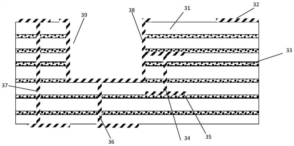
[0075] Such as image 3 As shown, it is a schematic diagram of the side metallization of the inner wall of the blind groove in this embodiment. The semi-finished product of the fourteen-layer microstrip board after lamination includes: seven-layer microwave dielectric board 31 based on perovskite ceramic filling with a dielectric constant of 10.20, adhesive material 33 (thermosetting adhesive film made of 2929 material), buried hole 34 , Through hole 37, inner pattern 35. According to the processing parameters in Table 1, the blind groove 39 and the blind hole 36 on the 12-piece 1 working board are obtained (12 pieces together are 12 semi-finished microstrip boards together), and the blind groove 39 is made by adhesive tape blocking glue opening method craft. The plasma treatment is performed on the through hole 37 and the blind groove 39 according to the parameters in Table 1. Then perform plasma microetching according to the parameters in Table 1, and then perform electro...


PUM

PropertyMeasurementUnit
Thicknessaaaaaaaaaa
Thicknessaaaaaaaaaa
Roughnessaaaaaaaaaa

Abstract

The invention discloses a multi-layer microstrip board processing method based on a perovskite ceramic filling substrate, and belongs to the technical field of microwave printed circuit board manufacturing, and the method comprises the steps: obtaining the inner wall or shape side wall of a blind groove through mechanical milling, sequentially carrying out the activation modification and micro-etching of the inner wall or shape side wall of the blind groove, and then carrying out the chemical copper plating and electrocoppering thickening, and finally, performing surface coating and plating, and obtaining the final product through appearance machining. According to the invention, the problems of low side edge processing precision, poor hydrophilicity, difficult deposition of a copper layer, easy generation of holes and cracking of a copper plating layer, poor adhesion after deposition, easy shedding and low reliability of a dielectric substrate according to a traditional multilayer microstrip plate processing method due to change of the filler proportion and variety are effectively solved, the roughness of the copper plating layer is less than or equal to 20 [mu] m, and the yield is improved, the thickness of the copper plating layer can reach 20 microns or above, and 95% or above of the copper plating layer is complete, compact and free of cracks.

Description

technical field [0001] The invention relates to the technical field of microwave printed circuit board manufacturing, in particular to a multilayer microstrip board processing method based on a perovskite ceramic filled substrate. Background technique [0002] Microstrip boards (microwave printed boards) are key basic materials for national defense wireless communication systems and microwave military electronic complete machines. They are widely used in core components such as digital array modules, antennas, and TR components. They are indispensable for active models and pre-research equipment. One of the indispensable electronic materials. With the rapid development of 5G communication technology, the demand for microstrip boards is growing exponentially. In order to reduce the dielectric loss of the signal in the high-frequency line and achieve the purpose of high-speed transmission, the first consideration of the microstrip board when selecting the substrate material i...

Claims


Application Information

Patent Timeline
IPC IPC(8): H05K3/46H05K3/42
CPCH05K3/46H05K3/424H05K2203/0346H05K2203/03
Inventor 朱春临程辉明邹嘉佳赵丹王璐
Owner CHINA ELECTRONIC TECH GRP CORP NO 38 RES INST
Why Eureka
Try Eureka