Preparation method of composite substrate, composite film and electronic component

A composite substrate and composite film technology, which is applied in the manufacturing of electrical components, piezoelectric devices/electrostrictive devices, semiconductor/solid-state devices, etc. Rough interface, increased substrate dielectric loss, etc.

Active Publication Date: 2021-02-26
JINAN JINGZHENG ELECTRONICS
View PDF18 Cites 1 Cited by
  • Summary
  • Abstract
  • Description
  • Claims
  • Application Information

AI Technical Summary

Problems solved by technology

[0004] This application provides a method for preparing a composite substrate, a composite thin film and electronic components to solve the problem of thermal oxidation directly on the polysilicon layer in the p

Method used


Image

  • Preparation method of composite substrate, composite film and electronic component
  • Preparation method of composite substrate, composite film and electronic component
  • Preparation method of composite substrate, composite film and electronic component

Examples


preparation example Construction

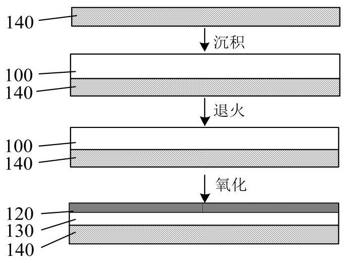
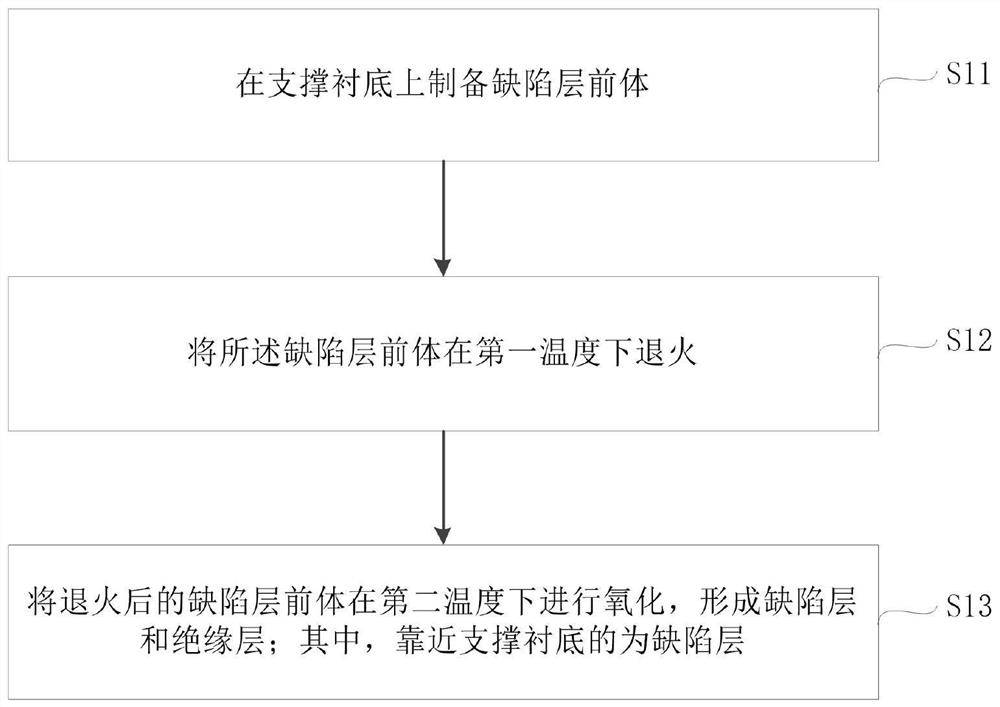
[0039] Specifically, refer to figure 2 , the preparation method comprises:

[0040] S11 , preparing a defect layer precursor 100 on the supporting substrate 140 .

[0041] Optionally, the preparation method of the defect layer precursor 100 is LPCVD or PECVD, and its thickness may be 200nm-20um, as long as it can realize the support function, which is not specifically limited.

[0042] Wherein, the LPCVD or PECVD is an existing method, for details, reference may be made to the implementation of an existing method, and no further description is given here.

[0043] S12, annealing the defect layer precursor 100 at a first temperature.

[0044] Optionally, in this step, the support substrate 140 containing the defect layer precursor 100 obtained in step S11 is placed in a high-temperature annealing furnace, and nitrogen annealing is performed at 900° C. to 1100° C. (first temperature), and the annealing time is 3h~24h.

[0045] Before the annealing, the wafer prepared in ste...

Embodiment 1

[0083] 1) A Si single wafer is selected as the support substrate, and a polysilicon layer with a thickness of 1.8um is grown on the support substrate by LPCVD as a defect layer precursor, and then the surface of the polysilicon layer is cleaned.

[0084] 2) Place the supporting substrate with the polysilicon layer in step 1) for annealing in a high-temperature annealing furnace, the annealing temperature is 1000°C, the annealing time is 8h, and it is cleaned.

[0085] 3) Perform thermal oxidation treatment on the annealed and cleaned polysilicon layer in step 2), the thermal oxidation temperature is 900°C, and the thermal oxidation time is 10h, and the part of the polysilicon layer far away from the supporting substrate is oxidized into silicon dioxide (insulating layer) , the part of the polysilicon close to the supporting substrate is not oxidized to form a defect layer. The surface of the silicon dioxide layer is planarized, and the planarized silicon dioxide surface is cle...

Embodiment 2

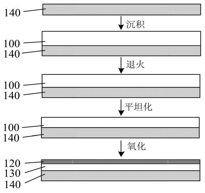
[0089] 1) A Si single wafer is selected as the support substrate, and a polysilicon layer with a thickness of 1.8um is grown on the support substrate by LPCVD as a defect layer precursor, and then the surface of the polysilicon layer is cleaned.

[0090] 2) Place the supporting substrate with the polysilicon layer in step 1) for annealing in a high-temperature annealing furnace, the annealing temperature is 1000°C, the annealing time is 8h, and it is cleaned.

[0091] 3) Polishing the annealed polysilicon layer in step 2), removing a thickness of 300 nm, and cleaning the surface of the polished polysilicon layer again.

[0092] 4) Perform thermal oxidation treatment on the polished and cleaned polysilicon layer in step 3), the thermal oxidation temperature is 900°C, the thermal oxidation time is 10h, and the part of the polysilicon layer far away from the supporting substrate is oxidized into silicon dioxide (insulating layer) , the part of the polysilicon close to the support...


PUM

PropertyMeasurementUnit
Thicknessaaaaaaaaaa
Thicknessaaaaaaaaaa
Thicknessaaaaaaaaaa

Abstract

The invention discloses a preparation method of a composite substrate, a composite film and an electronic component, and the preparation method of the composite substrate comprises the following steps: firstly, preparing a defect layer precursor on a support substrate; then, annealing the defect layer precursor at a first temperature; and oxidizing the annealed defect layer precursor at a second temperature to form a defect layer close to the support substrate and an insulating layer, so as to obtain the composite substrate. By the adoption of the scheme, annealing is conducted at the first temperature, crystalline grains in the defect layer precursor are fully reconstructed, and then the defect layer precursor is oxidized at the second temperature to prepare the insulating layer, so thatit is guaranteed that crystalline grain reconstruction does not happen to the defect layer precursor any more during long-time high-temperature oxidation; and further, the interface roughness of the defect layer and the insulating layer is reduced, the oxidation uniformity of the insulating layer is improved, and the dielectric loss of the composite substrate in use is reduced. The photoetching process of the composite substrate in subsequent use and the consistency of the finally manufactured device are not influenced.

Description

technical field [0001] The present application relates to the field of semiconductor technology, in particular to a method for preparing a composite substrate, a composite thin film and electronic components. Background technique [0002] Piezoelectric films used in surface acoustic wave filters generally include piezoelectric layers and substrate layers. Among them, the piezoelectric layer is a functional layer, and its function is to realize the mutual conversion between electricity and sound. The piezoelectric layer is usually lithium tantalate (LiTaO 3 , referred to as LT) or lithium niobate (LiNbO 3 , referred to as LN) piezoelectric single crystal structure, the substrate layer generally uses materials with high thermal conductivity, low thermal expansion coefficient and high Young's modulus to support the piezoelectric layer, improve heat dissipation performance and reduce temperature compensation coefficient. [0003] In the current relatively mature scheme, the su...

Claims


Application Information

Patent Timeline
IPC IPC(8): H01L41/08H01L41/22H01L21/02
CPCH03H9/02559H03H9/02574H03H9/02566H03H9/25H03H9/64H03H3/08
Inventor 杨超李真宇张秀全李洋洋
Owner JINAN JINGZHENG ELECTRONICS
Why Eureka
Try Eureka