Semiconductor laser

A semiconductor and laser technology, applied in the laser field, can solve the problems of high development cost, difficulty in achieving watt-level high power output, and complex design of built-in grating structure.

Active Publication Date: 2021-02-26
CHANGCHUN INST OF OPTICS FINE MECHANICS & PHYSICS CHINESE ACAD OF SCI
View PDF6 Cites 4 Cited by
  • Summary
  • Abstract
  • Description
  • Claims
  • Application Information

AI Technical Summary

Problems solved by technology

For example, the power amplifier of the master oscillator and the tapered laser obtain high power output through the tapered semiconductor optical amplifier, but the light output aperture of the tapered amplifier is usually above 100 microns, resulting in extremely low coupling efficiency with the single-mode fiber or single-mode waveguide
Another example is that a slab-coupled waveguide laser combines a specially designed epitaxial structure with a

Method used


Image

  • Semiconductor laser
  • Semiconductor laser
  • Semiconductor laser

Examples


Embodiment Construction

[0027]The technical solutions in the embodiments of the present invention will be clearly and completely described below in conjunction with the accompanying drawings in the embodiments of the present invention. Obviously, the described embodiments are only a part of the embodiments of the present invention, rather than all the embodiments. Based on the embodiments of the present invention, all other embodiments obtained by those of ordinary skill in the art without creative work shall fall within the protection scope of the present invention.

[0028]In order to enable those skilled in the art to better understand the solution of the present invention, the present invention will be further described in detail below with reference to the accompanying drawings and specific embodiments.

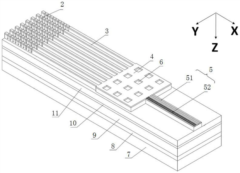
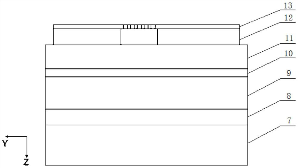
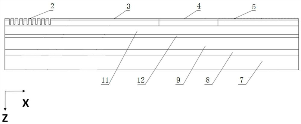
[0029]Please refer toFigure 1 to Figure 4,figure 1 Is a schematic diagram of the structure of a semiconductor laser provided by an embodiment of the present invention;figure 2 forfigure 1 Right viewimage 3...


PUM


Abstract

The invention discloses a semiconductor laser, which comprises a semiconductor PN junction, and a surface active Bragg reflection grating, a ridge-shaped waveguide array, a multimode interference waveguide and a super-symmetric array waveguide which are arranged on the semiconductor PN junction and distributed along the same column, the surface active Bragg reflection grating is arranged at one end of the ridge-shaped waveguide array, one end of the multimode interference waveguide is adjacent to the other end of the ridge-shaped waveguide array, and the super-symmetric array waveguide is adjacent to the other end of the multimode interference waveguide. According to the semiconductor laser, the surface active Bragg grating is used for providing single-frequency laser with tunable wavelength, the ridge-shaped waveguide array is used for gain amplification, the multimode interference waveguide is used for coherent coupling, and finally, the super-symmetric array waveguide is used for secondary transverse mode selection and gain. And high-power, narrow-linewidth and wavelength-tunable high-beam-quality laser is realized.

Description

Technical field[0001]The invention relates to the field of lasers, in particular to a semiconductor laser.Background technique[0002]Semiconductor lasers are laser devices that use semiconductor materials as working materials. They have the advantages of small size, light weight, direct electro-optical conversion, high conversion efficiency, good beam quality, and narrow laser line width. They are used in optical phased array lidar, active detection and recognition, etc. The field has a wide range of application prospects.[0003]The existing tunable, high beam quality semiconductor lasers mainly include waveguide mode selection single-tube devices such as master-controlled oscillator power amplifiers, tapered lasers, plate-coupled waveguide lasers, distributed feedback lasers, and distributed Bragg reflection lasers.[0004]Although high beam quality semiconductor lasers have made great progress in improving output power, beam quality, and optimizing spectral linewidth, various types of...

Claims


Application Information

Patent Timeline
IPC IPC(8): H01S5/183H01S5/22
CPCH01S5/18386H01S5/22
Inventor 贾鹏梁磊陈泳屹秦莉宁永强王立军
Owner CHANGCHUN INST OF OPTICS FINE MECHANICS & PHYSICS CHINESE ACAD OF SCI
Why Eureka
Try Eureka