

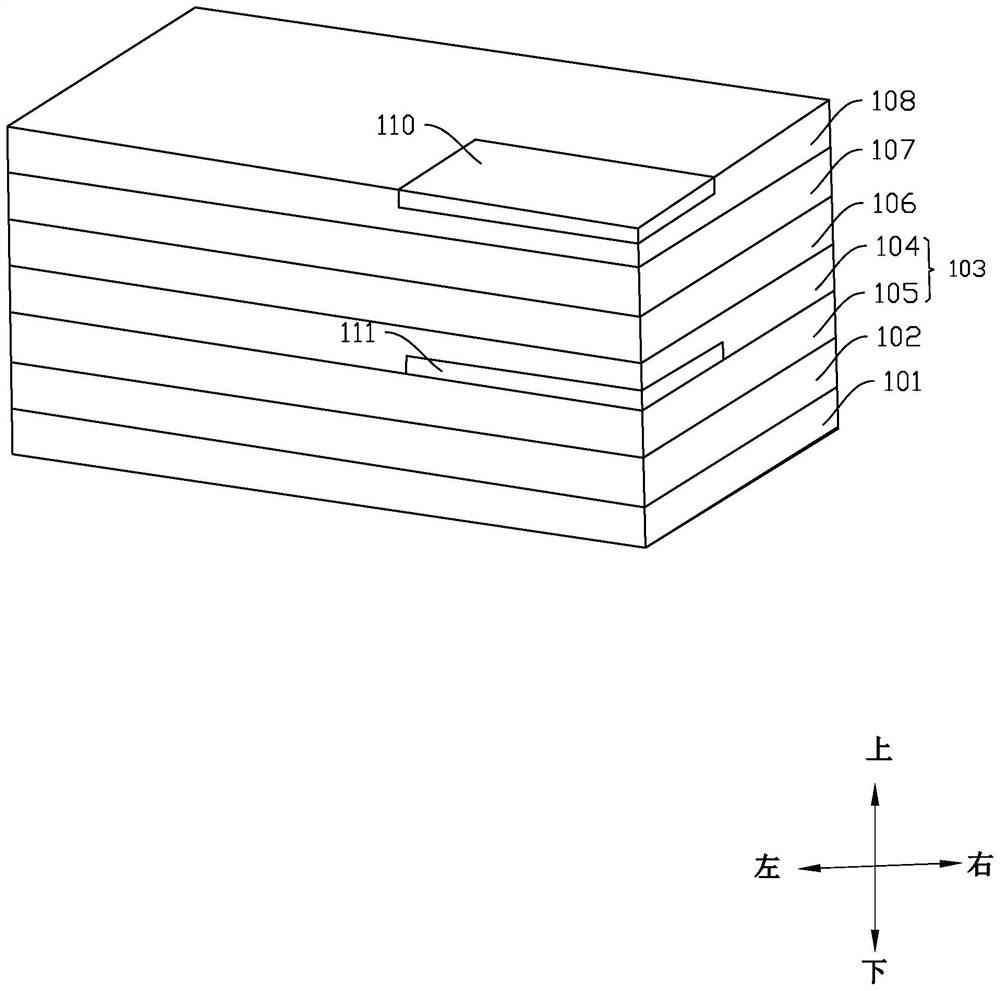
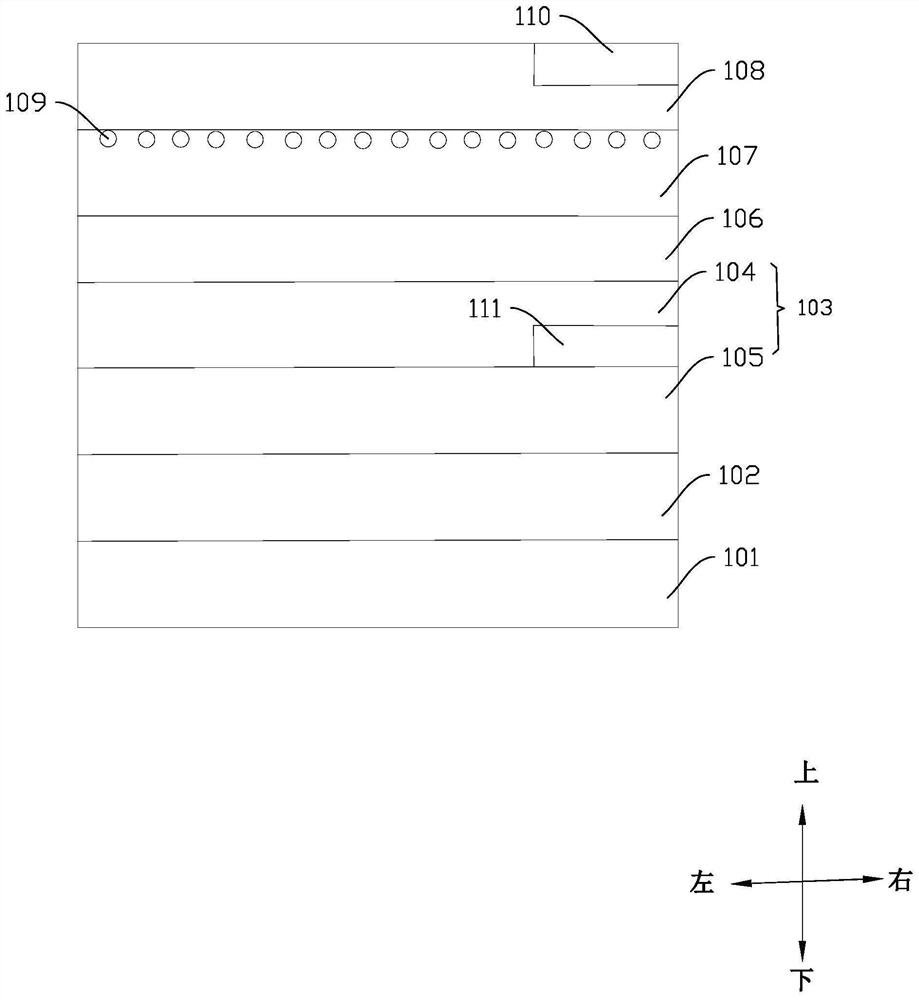
GaN-based epitaxial wafer structure
An epitaxial wafer, N-type semiconductor technology, applied in electrical components, circuits, semiconductor devices, etc., can solve the problems of difficult formation, low efficiency, lattice mismatch, etc., to achieve the effect of improving luminous efficiency
- Summary
- Abstract
- Description
- Claims
- Application Information
AI Technical Summary
Problems solved by technology
Method used
Image

Examples
Embodiment Construction
[0022] Embodiments of the present invention are described in detail below, examples of which are shown in the drawings, wherein the same or similar reference numerals designate the same or similar elements or elements having the same or similar functions throughout. The embodiments described below by referring to the figures are exemplary only for explaining the present invention and should not be construed as limiting the present invention.
[0023] In the description of the present invention, it should be understood that the orientation descriptions, such as up, down, front, back, left, right, etc. indicated orientations or positional relationships are based on the orientations or positional relationships shown in the drawings, and are only In order to facilitate the description of the present invention and simplify the description, it does not indicate or imply that the device or element referred to must have a specific orientation, be constructed and operated in a specific ...
PUM
| Property | Measurement | Unit |
|---|---|---|
| thickness | aaaaa | aaaaa |
| thickness | aaaaa | aaaaa |
| thickness | aaaaa | aaaaa |
Abstract
Description
Claims
Application Information