Up-conversion low-turn-on voltage infrared detection-light emitting device and preparation method thereof
A technology of turn-on voltage and infrared detection, which is applied in the direction of electric solid-state devices, semiconductor/solid-state device manufacturing, electrical components, etc., can solve the problems of turn-on voltage and low light-to-light conversion efficiency, and achieve lower turn-on voltage and weak light detection capabilities Improved effect
- Summary
- Abstract
- Description
- Claims
- Application Information
AI Technical Summary
Problems solved by technology
Method used
Image
Examples
Embodiment 1
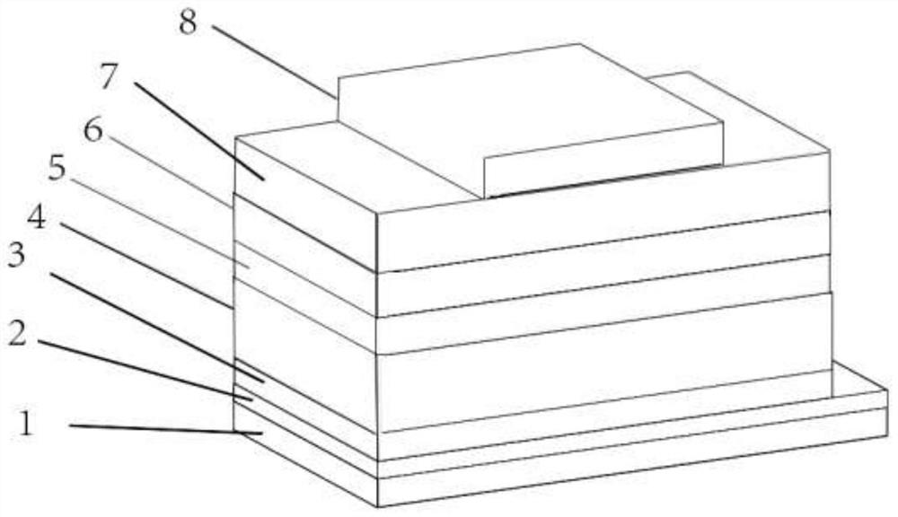
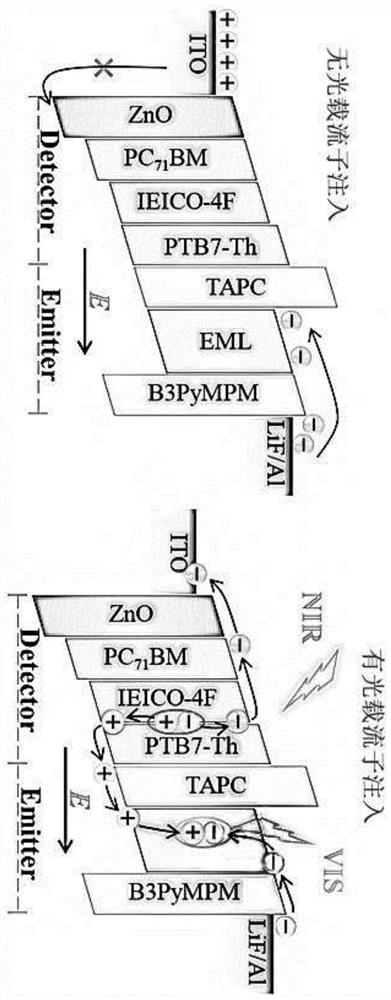
[0040] Such as figure 1 As shown, in Example 1, an up-conversion low turn-on voltage infrared detection-light-emitting device, the device device includes a transparent substrate 1, a transparent conductive film 2, a first electron transport layer 3, and a ternary active layer from bottom to top. 4. Hole transport layer 5, light-emitting layer 6, second electron transport layer 7, top electrode 8; ternary active layer 4 is a binary electron donor-acceptor active layer doped with a third element acceptor material, and Annealing is used to form a thin film with a crystallographic orientation in the plane transport direction; the light-emitting host material of the second electron transport layer 7 and the light-emitting layer 6 forms an exciplex at the interface between the second electron transport layer 7 and the light-emitting layer 6 . Specifically, the transparent conductive film 2 is specifically ITO conductive glass; the first electron transport layer 3 is specifically zin...
Embodiment 2
[0049] This embodiment has the same inventive concept as Embodiment 1. On the basis of Embodiment 1, a method for preparing an up-conversion low-turn-on-voltage infrared detection-light-emitting device is provided. The method includes the following steps:
[0050] S01: Perform patterned etching on the transparent conductive film 2 with the transparent substrate 1 after cleaning, leave an electrical test channel, and enter step S02; wherein, use transparent cleaning agent, acetone, ethanol, and deionized water to clean in sequence Transparent substrate 1, transparent conductive film 2, transparent conductive film 2 is ITO conductive glass.
[0051] S02: The first electron transport layer 3 is prepared by spin coating by solution method, and then the third element acceptor material is mixed into the binary electron donor-acceptor active layer and dissolved in chlorobenzene and chloronaphthalene for spin coating, spin coating After the annealing treatment is completed, the prepar...
PUM
| Property | Measurement | Unit |
|---|---|---|
| Thickness | aaaaa | aaaaa |
| Thickness | aaaaa | aaaaa |
| Thickness | aaaaa | aaaaa |
Abstract
Description
Claims
Application Information


