Up-conversion low turn-on voltage infrared detection-light-emitting device and preparation method thereof

A technology of turn-on voltage and infrared detection, which is applied in the direction of electric solid-state devices, semiconductor/solid-state device manufacturing, electrical components, etc., can solve the problems of turn-on voltage and low light-to-light conversion efficiency, and achieve lower turn-on voltage and weak light detection capabilities Improve and reduce quenching effect

Active Publication Date: 2022-08-02
UNIV OF ELECTRONICS SCI & TECH OF CHINA
View PDF2 Cites 0 Cited by
  • Summary
  • Abstract
  • Description
  • Claims
  • Application Information

AI Technical Summary

Problems solved by technology

[0007] The purpose of the present invention is to overcome the problems of low light-to-light conversion efficiency and high turn-on voltage of existing single-layer infrared up-conversion devices, and provide an up-conversion low-turn-on voltage infrared detection-light-emitting device and its preparation method

Method used


Image

  • Up-conversion low turn-on voltage infrared detection-light-emitting device and preparation method thereof
  • Up-conversion low turn-on voltage infrared detection-light-emitting device and preparation method thereof
  • Up-conversion low turn-on voltage infrared detection-light-emitting device and preparation method thereof

Examples


Embodiment 1

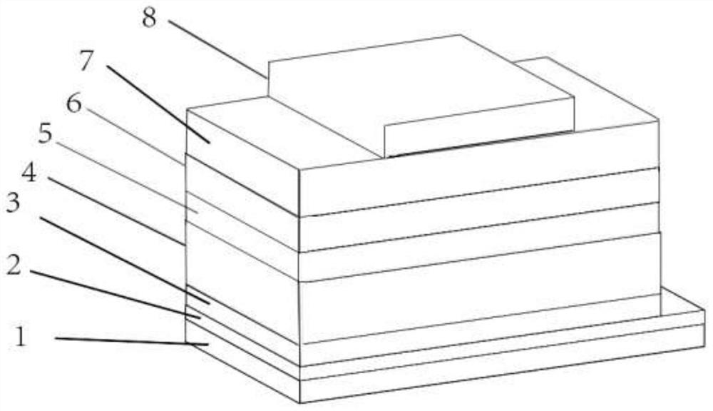
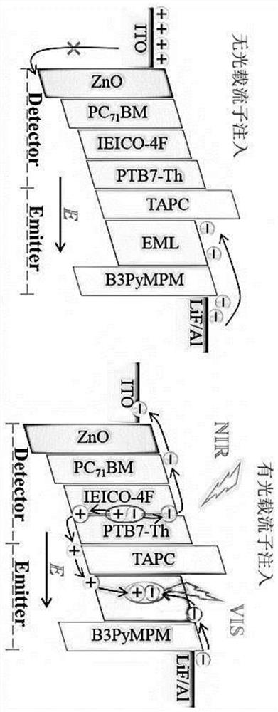
[0040] like figure 1 As shown, in Example 1, an up-conversion low turn-on voltage infrared detection-light-emitting device, the device device includes a transparent substrate 1, a transparent conductive film 2, a first electron transport layer 3, a ternary active layer from bottom to top 4. The hole transport layer 5, the light-emitting layer 6, the second electron transport layer 7, and the top electrode 8; A thin film with crystal orientation in the plane transport direction is formed by annealing; the light-emitting host material of the second electron transport layer 7 and the light-emitting layer 6 forms an excimer complex at the interface between the second electron transport layer 7 and the light-emitting layer 6 . Specifically, the transparent conductive film 2 is ITO conductive glass; the first electron transport layer 3 is zinc oxide; the hole transport layer 5 is TAPC, with a thickness ranging from 20 to 40 nm, preferably 30 nm; the top electrode 8 is LiF / Al compos...

Embodiment 2

[0049] This embodiment has the same inventive concept as Embodiment 1. On the basis of Embodiment 1, a method for preparing an up-conversion low-on-voltage infrared detection-light-emitting device is provided, and the method includes the following steps:

[0050] S01: performing patterned etching on the cleaned transparent conductive film 2 with the transparent substrate 1, leaving an electrical test channel, and entering step S02; wherein, successively use a transparent cleaning agent, acetone, ethanol, and deionized water for cleaning The transparent substrate 1, the transparent conductive film 2, and the transparent conductive film 2 are ITO conductive glass.

[0051] S02: Prepare the first electron transport layer 3 by solution spin coating, and then mix the tertiary acceptor material in the binary electron donor-acceptor active layer and dissolve it in chlorobenzene and chloronaphthalene for spin coating, spin coating After the annealing treatment is completed, the prepar...


PUM

PropertyMeasurementUnit
thicknessaaaaaaaaaa
thicknessaaaaaaaaaa
thicknessaaaaaaaaaa

Abstract

The invention discloses an up-conversion low turn-on voltage infrared detection-light-emitting device and a preparation method thereof, belonging to the technical field of infrared up-conversion detection. The device comprises a transparent substrate, a transparent conductive film, a first electron transport layer, three A primary active layer, a hole transport layer, a light-emitting layer, a second electron transport layer, and a top electrode; the ternary active layer is a binary electron donor-acceptor active layer doped with a tertiary acceptor material, and formed by annealing A thin film with crystal orientation in the plane transport direction; the light-emitting host material of the second electron transport layer and the light-emitting layer forms an excimer complex at the interface between the second electron transport layer and the light-emitting layer. The light-emitting layer and the second electron transport layer use the interface organic excimer composite luminescence and the ternary active layer to form a thin film with crystal orientation in the plane transmission direction, which will greatly reduce the turn-on voltage, reduce the overall energy consumption of the device, and improve the detection sensitivity of the device's infrared up-conversion. In the fields of near-infrared detection and imaging, infrared light source calibration, infrared identification, etc.

Description

technical field [0001] The invention relates to the technical field of infrared up-conversion detection, in particular to an up-conversion low turn-on voltage infrared detection-light-emitting device and a preparation method thereof. Background technique [0002] Infrared up-conversion detectors can convert invisible infrared light into visible light emitted by the human eye. This converted luminescence detection has great application prospects in infrared imaging, environmental monitoring, and military fields. Traditional infrared detection devices require arrays and back-end image processing circuits for imaging, and their resolution is also related to the number of arrays, which greatly limits their functions and fabrication difficulties. Infrared up-conversion detectors, however, only need a larger-area device to achieve such functions, and their resolution can theoretically be close to the size of the smallest film. [0003] The infrared up-conversion device is compose...

Claims


Application Information

Patent Timeline
Patent Type & Authority Patents(China)
IPC IPC(8): H01L27/30H01L27/32H01L51/50H01L51/54H01L51/56
CPCH10K39/30H10K59/60H10K85/10H10K85/60H10K50/11H10K2101/40H10K50/12H10K71/00
Inventor 王军韩嘉悦杜晓扬何泽宇陶斯禄蒋亚东
Owner UNIV OF ELECTRONICS SCI & TECH OF CHINA
Why Eureka
Try Eureka