Novel BHT and HT matched high-performance OLED device
An electroluminescent device and energy level technology, which is applied in the fields of electro-solid devices, semiconductor devices, semiconductor/solid-state device manufacturing, etc. Poor and other problems
- Summary
- Abstract
- Description
- Claims
- Application Information
AI Technical Summary
Problems solved by technology
Method used
Image
Examples
preparation Embodiment 1
[0094] Anode interface buffer layer 1: Use the OLED Chuster Deposition System (manufacturer: CHOSHU INDUSTRY Co.LTD.) evaporation equipment model 1504-10117-01-0 to place the hole transport host material BHT106 and the P-type dopant material P1 on the In two different evaporation sources, at a vacuum of 1.0E -5 Under Pa pressure, control the evaporation rate of BHT106 as Control the evaporation rate of P1 as Co-evaporated to obtain the anode interface buffer layer HI1 of the present invention.
[0095] Anode interface buffer layer 2: Repeat the preparation process of HI preparation example 1, except that the P-type dopant material P1 is replaced by P2 to obtain the anode interface buffer layer HI2.
[0096] Anode interface buffer layer 3: Repeat the preparation process of HI preparation example 1, the difference is that the main hole transport material BHT106 is replaced by BHT112 to obtain an anode interface buffer layer HI3.
[0097] Anode interface buffer layer 4: Repe...
Embodiment 1
[0103] Vacuum evaporation is carried out under the following conditions: use the OLED ChusterDeposition System (manufacturer: CHOSHU INDUSTRYCo.LTD.) evaporation equipment of model 1504-10117-01-0, at a vacuum degree of 1.0E -5 Under the pressure of Pa, the evaporation rate is controlled as
Embodiment 1
[0104] Device Preparation Example 1: Carry out according to the following process:
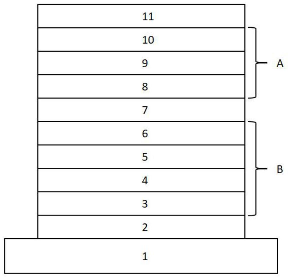
[0105] a) Use transparent glass as the substrate, and coat it with ITO with a thickness of 150nm as the anode layer, then use deionized water, acetone, and ethanol to ultrasonically clean each for 15 minutes, and then treat it in a plasma cleaner for 2 minutes;
[0106] b) On the washed first electrode layer, vapor-deposit the anode interface buffer layer 1 obtained in Example 1 by a vacuum evaporation method, with a thickness of 5 nm;
[0107] c) On the anode interface buffer layer, a hole transport layer is evaporated by vacuum evaporation, the material of the first hole transport layer is BH106, the material of the second hole transport layer is HT305, and the total thickness is 100nm;
[0108] d) Evaporating an electron blocking layer EB1 on the hole transport layer by vacuum evaporation with a thickness of 10 nm;
[0109] e) On the electron blocking layer, evaporate the light-emitting la...
PUM
| Property | Measurement | Unit |
|---|---|---|
| thickness | aaaaa | aaaaa |
| thickness | aaaaa | aaaaa |
| thickness | aaaaa | aaaaa |
Abstract
Description
Claims
Application Information


