Organic single-crystal semiconductor structure and preparation method thereof

A single crystal semiconductor, organic semiconductor technology, applied in semiconductor/solid-state device manufacturing, semiconductor devices, electrical solid-state devices, etc., to achieve efficient extraction and injection, and overcome the effects of transmission traps/defects

Active Publication Date: 2021-03-19
ZHEJIANG UNIV
View PDF5 Cites 1 Cited by
  • Summary
  • Abstract
  • Description
  • Claims
  • Application Information

AI Technical Summary

Problems solved by technology

Based on the problems existing in the prior art, the inventors, after a lot of research and unremitting efforts, overcame the obstacles of the prior art and academic thinking patterns, and unexpectedly successfully prepared a uniformly grown, highly effective The organic semiconductor single crystal thin film with uniform growth and full cov

Method used


Image

  • Organic single-crystal semiconductor structure and preparation method thereof
  • Organic single-crystal semiconductor structure and preparation method thereof
  • Organic single-crystal semiconductor structure and preparation method thereof

Examples


Embodiment 1

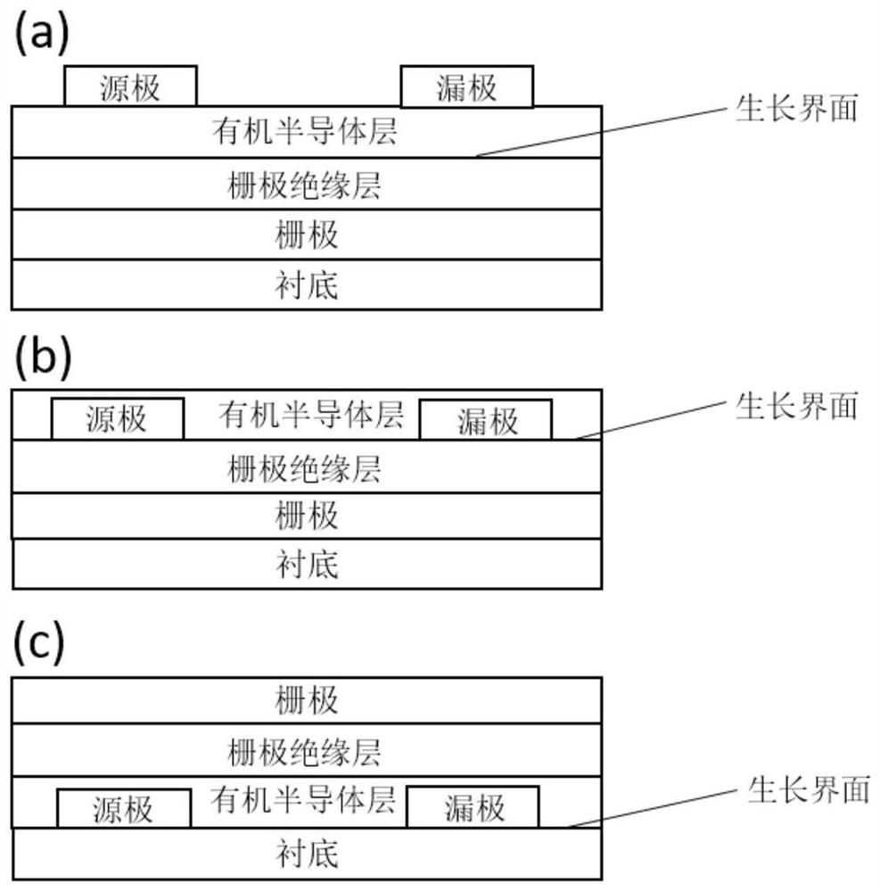
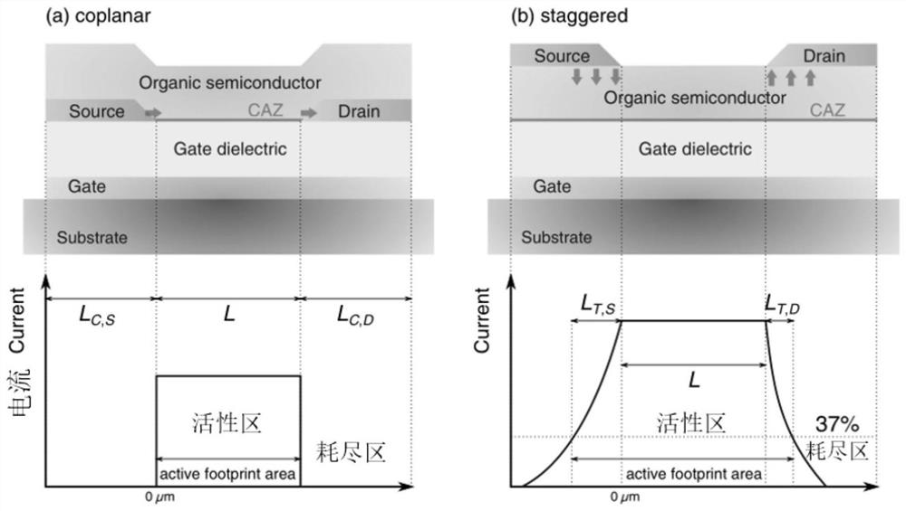
[0126] Example 1: A bottom-contact organic single crystal semiconductor structure based on 6,13-bis(triisopropylsilylethynyl)pentacene (TIPS-pentacene) and a top-gate bottom-contact structure based on this The preparation method of the field effect transistor device, comprises the following steps:

[0127] (1) Take a P-type silicon wafer with a thickness of 575 μm. There is a 300 nm thick silicon dioxide insulating layer on the silicon wafer, and spin-coat cross-linked polystyrene on the silicon substrate to prepare an auxiliary growth layer;

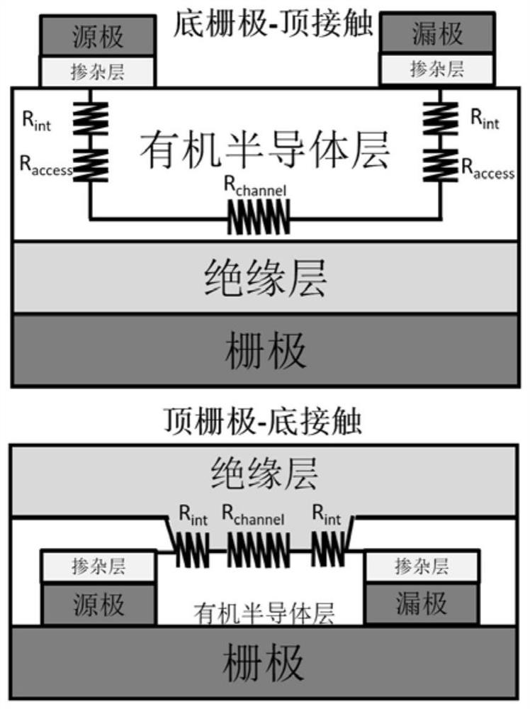
[0128] (2) On the initial film prepared in step (1), a long strip of Au with a thickness of about 30 nm is deposited by thermal evaporation under high vacuum as the source and drain electrodes, and the upper surface of the auxiliary growth layer is in contact with the lower surface of the electrode , the contact mode is the upper type;

[0129] (3) Regulate the temperature of the growth environment to be 20±1°C, and the humidity to be...

Embodiment 2

[0136] Example 2: A bottom-contact organic single crystal semiconductor structure based on 6,13-bis(triisopropylsilylethynyl)pentacene (TIPS-pentacene) and a top-gate bottom-contact structure based on this Fabrication methods of field effect transistor devices.

[0137] Refer to Example 1 for the preparation method of the field effect transistor device in Example 2, and the formula and process parameters are shown in Table 1 and Table 2. The structure and performance characterization methods are the same as those in Example 1. The obtained device properties are shown in Table 4.

Embodiment 3

[0138] Example 3: A bottom-contact organic single crystal semiconductor structure based on 6,13-bis(triisopropylsilylethynyl)pentacene (TIPS-pentacene) and a top-gate bottom-contact structure based on this Fabrication methods of field effect transistor devices.

[0139] Refer to Example 1 for the preparation method of the field effect transistor device of Example 3, and the formula and process parameters are shown in Table 1 and Table 2. The structure and performance characterization methods are the same as those in Example 1. The obtained device properties are shown in Table 4.


PUM

PropertyMeasurementUnit
Hole mobilityaaaaaaaaaa

Abstract

The invention discloses an organic single-crystal semiconductor structure and a preparation method thereof. The organic single-crystal semiconductor structure comprises a substrate, and an auxiliary growth layer, an electrode and an organic single-crystal semiconductor layer which are deposited on the substrate from bottom to top, and the organic single-crystal semiconductor layer is an organic semiconductor single-crystal thin film with basically unchanged morphology before and after crossing the electrode, and the organic semiconductor single-crystal thin film can realize full coverage on abottom contact type substrate with any shape and any size, so that an approximately ideal morphology on an industrial scale is obtained. The organic single-crystal semiconductor structure can be usedas a key part of an organic field effect transistor to realize rapid transmission of carriers. On the basis of the semiconductor structure, the invention further provides an organic field effect transistor device which is convenient to prepare and efficient in performance, and has a good application prospect in the field of organic photoelectricity.

Description

technical field [0001] The invention relates to the field of organic semiconductors, in particular to an organic single crystal semiconductor structure and a preparation method thereof. Background technique [0002] Organic semiconductor devices have attracted widespread attention in the field of semiconductor devices because of their light weight, low price, flexibility, and large-area fabrication. The emerging new technologies have greatly promoted the development of organic photoelectric semiconductor devices such as organic solar cells, organic light-emitting diodes, and organic field-effect transistors. Among them, the structure of the device is one of the keys to realize high-efficiency photoelectric functions. Taking the structure of the organic field effect transistor as an example, the organic field effect transistor is mainly composed of the following parts: ① electrode, which can be divided into source and source according to the different access voltage Electrod...

Claims


Application Information

Patent Timeline
IPC IPC(8): H01L51/05H01L51/40
CPCH10K71/12H10K10/464H10K10/466H10K85/623H10K85/654H10K85/40H10K10/484H10K71/20H10K71/40H10K10/00H10K50/00H10K71/15
Inventor 伍瑞菡李寒莹
Owner ZHEJIANG UNIV
Why Eureka
Try Eureka