Circuit structure with anti-laser joint filling layer and manufacturing method of circuit structure

A technology of circuit structure and caulking layer, which is applied in the fields of printed circuit manufacturing, printed circuit, printed circuit components, etc., can solve problems such as incomplete curing of solder resist materials, excessive etching, damaged circuit boards, etc., and achieve flatness of window walls Excellent, improved over-etching, and reduced material costs

Pending Publication Date: 2021-03-26
李家铭
View PDF0 Cites 0 Cited by
  • Summary
  • Abstract
  • Description
  • Claims
  • Application Information

AI Technical Summary

Problems solved by technology

However, when the solder mask is cured by light, because the reflectivity and thickness of the solder mask itself affect the penetration of UV light or visible light, the solder mask material at the bottom of the solder mask is not completely cured and is removed by a special chemical solvent
In this way, the problem of over-etching (overcut) is likely to occur during the development process, resulting in the exposure of the circuit layer that should be protected by the solder mask layer. When the subsequent soldering process is performed, it is likely to cause a short circuit or even damage the circuit board.
On the other hand, in the subsequent soldering process, short-circuits are likely to occur between adjacent pads due to too small spacing

Method used


Image

  • Circuit structure with anti-laser joint filling layer and manufacturing method of circuit structure
  • Circuit structure with anti-laser joint filling layer and manufacturing method of circuit structure
  • Circuit structure with anti-laser joint filling layer and manufacturing method of circuit structure

Examples


Embodiment Construction

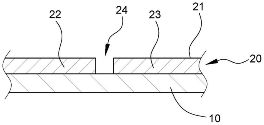
[0022] The circuit structure of the present application can be a single-layer board structure or a multi-layer composite board structure, which can be a carrier board of a flexible printed circuit board (Flexible Printed Circuit, FPC) or a carrier board of a rigid circuit board (Printed Circuit Board, PCB), The material used may be but not limited to polyethylene terephthalate (PET) or other polyester films, polyimide films, polyamideimide films, polypropylene films, polystyrene films.

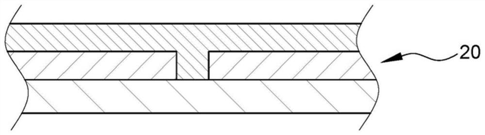
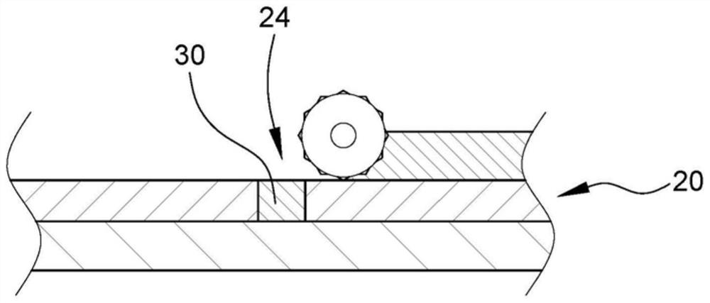
[0023] Please refer to figure 1 , in the first embodiment of the present application, a circuit layer 20 with a working surface 21 is first formed on a substrate 10. For example, a thin copper foil may be formed on the substrate 10 and then copper-plated to form The copper conductive layer is then imaged by the circuit image transfer technology to form the circuit layer 20 as mentioned above. The circuit layer 20 has a first pad 22 and a second pad 23 with a gap 24 therebetween. The first a...


PUM


Abstract

The invention provides a circuit structure with an anti-laser joint filling layer. The circuit structure comprises a substrate, a circuit layer, a joint filling layer and an anti-welding layer, the circuit layer is formed on the substrate, the circuit layer is provided with a first welding pad and a second welding pad, the joint filling layer is filled between the first welding pad and the secondwelding pad, the anti-welding layer partially covers the circuit layer, and the anti-welding layer is provided with an anti-welding window. At least one part of the first welding pad, at least one part of the second welding pad and at least one part of the joint filling layer are exposed in the solder mask window; and the thickness of the solder mask layer which can be burnt through by the laser beams in unit time is greater than the thickness of the joint filling layer which can be burnt through by the laser beams with the same intensity in unit time.

Description

technical field [0001] The present application relates to a method for manufacturing a circuit board, especially a method for manufacturing a circuit board with a window area. Background technique [0002] The traditional circuit board structure usually forms a solder mask layer on the metal circuit layer to cover the circuits and metal surfaces that do not need to be soldered, so as to prevent short circuits during soldering and save the amount of solder; on the other hand, the solder mask layer It can prevent water vapor and electrolyte from entering the circuit board, so as to avoid the oxidation of the circuit layer and endanger the electrical properties, and also prevent the equipment from damaging the circuit layer; The solder layer also provides insulation between adjacent circuits. [0003] Next, the solder resist layer on the designated soldering point of the circuit layer is removed by developing and etching process, so that the circuit layer of the soldering poin...

Claims


Application Information

Patent Timeline
IPC IPC(8): H05K1/02H05K3/00H05K3/28
CPCH05K1/02H05K3/0032H05K3/282
Inventor 李家铭
Owner 李家铭
Why Eureka
Try Eureka