Image sensor and manufacturing method thereof

A technology of an image sensor and a manufacturing method, which is applied to electric solid-state devices, semiconductor devices, radiation control devices, etc., can solve problems such as leakage and low efficiency, and achieve the effects of improving isolation efficiency and reducing dark current.

Pending Publication Date: 2021-04-02
WUHAN XINXIN SEMICON MFG CO LTD
View PDF11 Cites 0 Cited by
  • Summary
  • Abstract
  • Description
  • Claims
  • Application Information

AI Technical Summary

Problems solved by technology

However, STI as an isolation will cause a lot of damage and charge accumulation to the substrate due to the etching process, and then bring a dark current source; while the inverse IMP usually implants ions deeper in order to prevent dark current in the direction of the substrate. In order to increase the withstand voltage of the device, the efficiency of the doped region formed as an isolation is not high, and there will be a problem of leakage

Method used


Image

  • Image sensor and manufacturing method thereof
  • Image sensor and manufacturing method thereof
  • Image sensor and manufacturing method thereof

Examples


Embodiment Construction

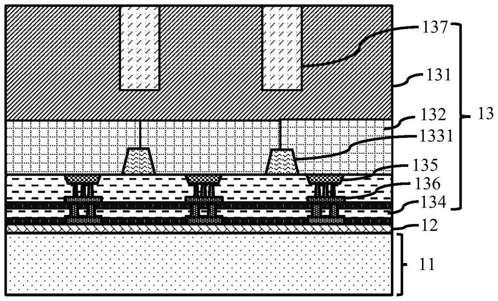
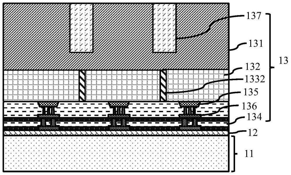
[0050] by Figure 1a ~ Figure 1b shown in the existing image sensor structure as an example, and Figure 1a ~ Figure 1b Shown is the structure of a back-illuminated image sensor, where, Figure 1a Each pixel in the shown image sensor is isolated by a shallow trench isolation structure, Figure 1b The pixel points in the image sensor shown are separated by doping regions formed by inversion ion implantation. From Figure 1a and Figure 1b It can be seen from the figure that the front side of the carrier wafer 11 and the device wafer 13 are bonded through the bonding layer 12, and the device wafer 13 includes a substrate 131 and a plurality of pixel unit regions 132 (ie, pixel points) located on the front side of the substrate 131 , a dielectric layer 134 formed on the pixel unit area 132, a transistor structure 135 and a metal interconnection structure 136 formed in the dielectric layer 134, and a deep trench isolation structure 137 is also formed in the substrate 131 on the ...


PUM


Abstract

The invention provides an image sensor and a manufacturing method thereof. The manufacturing method of the image sensor comprises the following steps: providing a substrate which comprises a pluralityof pixel unit regions and isolation regions located among the pixel unit regions; performing secondary ion implantation on the isolation regions; and performing high-temperature annealing processingon the substrate to form isolation layers in the isolation regions. According to the above technical scheme of the invention, the isolation efficiency is improved while dark current in the image sensor is reduced.

Description

technical field [0001] The invention relates to the field of semiconductor integrated circuit manufacturing, in particular to an image sensor and a manufacturing method thereof. Background technique [0002] An image sensor refers to a device that converts optical signals into electrical signals. According to different principles, it can be divided into CCD (Charge Coupled Device, Charge Coupled Device) image sensor and CMOS (Complementary Metal-Oxide Semiconductor, metal oxide semiconductor element) image sensor. Since the CMOS image sensor is manufactured using a traditional CMOS circuit process, the image sensor and its required peripheral circuits can be integrated, so that the CMOS image sensor has a wider application prospect. [0003] CMOS image sensors can be classified into front-illuminated image sensors and back-illuminated image sensors according to the location where light is received. Among them, the front-illuminated image sensor receives light from the fron...

Claims


Application Information

Patent Timeline
Patent Type & Authority Applications(China)
IPC IPC(8): H01L27/146
CPCH01L27/1463H01L27/14632H01L27/14687H01L27/14683
Inventor 薛广杰
Owner WUHAN XINXIN SEMICON MFG CO LTD
Why Eureka
Try Eureka