Array substrate, preparation method thereof and display device

A technology of array substrates and substrate substrates, which is applied in semiconductor/solid-state device manufacturing, electrical components, transistors, etc., can solve the problems of poor reliability of oxide semiconductor thin film transistors, avoid the impact of etching, improve reliability, and avoid being affected by damage effect

Pending Publication Date: 2021-04-02
HEFEI VISIONOX TECH CO LTD
View PDF3 Cites 1 Cited by
  • Summary
  • Abstract
  • Description
  • Claims
  • Application Information

AI Technical Summary

Problems solved by technology

[0005] The technical problem to be solved by the present invention is to overcome the problem of poor reliability of oxide semiconductor thin film transistors in the prior art

Method used


Image

  • Array substrate, preparation method thereof and display device
  • Array substrate, preparation method thereof and display device
  • Array substrate, preparation method thereof and display device

Examples


Embodiment Construction

[0064] As mentioned in the background art, the threshold voltage of the thin film transistors of the array substrate in the prior art will be severely shifted negatively.

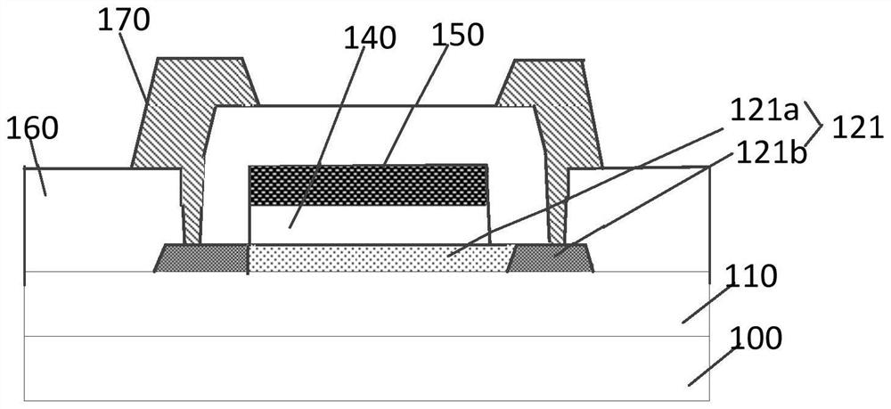
[0065] A kind of array substrate in the prior art, refer to figure 1 , including: a base substrate 100; an insulating layer 110 located on the base substrate 100; a thin film transistor located on a side of a part of the insulating layer 110 facing away from the base substrate 100, the thin film transistor is a top gate structure, and the thin film Transistor comprises: active layer 121, and the material of active layer 121 is indium gallium zinc oxide (IGZO), and described active layer 121 comprises channel region 121a and source drain region 121b; The top gate dielectric layer 140 on the side of the base substrate 100 ; the top gate layer 150 on the side of the top gate dielectric layer 140 facing away from the base substrate 100 ; the interlayer dielectric layer 160 and the source-drain conductive connec...


PUM

PropertyMeasurementUnit
thicknessaaaaaaaaaa
thicknessaaaaaaaaaa
thicknessaaaaaaaaaa

Abstract

The invention discloses an array substrate and a preparation method thereof, and a display device. The array substrate comprises a substrate body, an oxide semiconductor thin film transistor arrangedon the substrate body, comprising an oxide semiconductor active layer comprising a channel region and source and drain regions located on the two sides of the channel region, and a hydrogen-containinglayer in contact with the source and drain regions and being suitable for diffusing hydrogen into the source and drain regions. The array substrate can improve the reliability.

Description

technical field [0001] The present invention relates to the field of display technology, in particular to an array substrate, a preparation method thereof, and a display device. Background technique [0002] With the advancement of the information society, display devices are widely used. The display device includes a liquid crystal display device, a plasma display panel device, an organic light emitting diode display device, and the like. [0003] Among them, the liquid crystal display device and the organic light emitting diode display device include thin film transistors for electrically connecting pixel regions. Thin film transistors are used to drive pixel areas to display images. The thin film transistor includes an active layer, a source, a drain, a gate dielectric layer, and a gate, wherein the material of the active layer includes one of amorphous silicon, polysilicon, and oxide semiconductor materials. The conductivity when the material of the active layer is an...

Claims


Application Information

Patent Timeline
Patent Type & Authority Applications(China)
IPC IPC(8): H01L29/786H01L29/423H01L27/12H01L21/34
CPCH01L29/78606H01L29/78618H01L29/42364H01L29/42356H01L27/1225H01L29/66969H01L2029/42388
Inventor 曹曙光
Owner HEFEI VISIONOX TECH CO LTD
Why Eureka
Try Eureka