
Narrow-linewidth external cavity semiconductor laser linear array based on diffraction grating array

A diffraction grating and semiconductor technology, applied in semiconductor lasers, semiconductor laser optical devices, lasers, etc., can solve the problems of increased optical components, low output power, complex optical path adjustment, etc., to improve device stability and reduce spectral line width. , The effect of simplifying the optical path structure

Pending Publication Date: 2021-04-02
浙江长芯光电科技有限公司
View PDF0 Cites 0 Cited by
  • Summary
  • Abstract
  • Description
  • Claims
  • Application Information

AI Technical Summary

Problems solved by technology

The disadvantage of this scheme is that due to the grating Littmann structure, when the light is reflected by the feedback mirror and enters the grating again, the first-order diffracted light is fed back to the laser, and the zero-order diffracted light is lost, so the output power is low
In addition, due to the introduction of the feedback mirror, the number of optical elements increases, so the adjustment of the optical path is complicated and difficult to adjust
Patent No. 2007200944437 The diffraction grating array external cavity semiconductor laser line array has the problems of complex structure of the diffraction grating array external cavity semiconductor laser line array, many optical path components, and spectral broadening of the line array

Method used


Image

  • Narrow-linewidth external cavity semiconductor laser linear array based on diffraction grating array
  • Narrow-linewidth external cavity semiconductor laser linear array based on diffraction grating array
  • Narrow-linewidth external cavity semiconductor laser linear array based on diffraction grating array

Examples


Embodiment

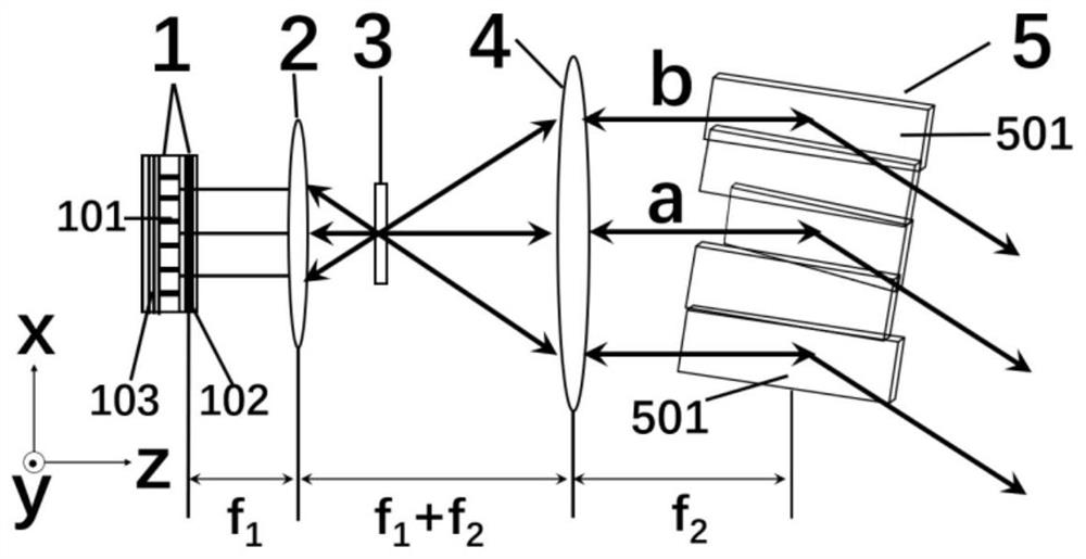
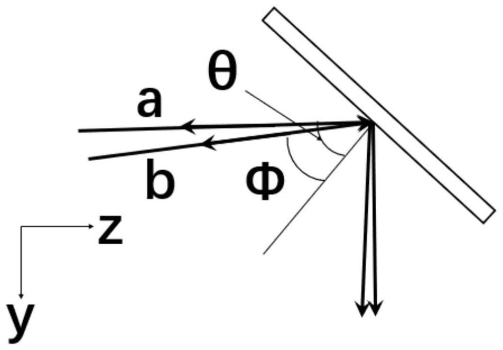
[0020] Such as figure 2 , image 3 , Figure 4 As shown, the narrow-linewidth external-cavity semiconductor laser bar array based on the diffraction grating array includes a semiconductor laser bar array 1, and the semiconductor laser bar array 1 is composed of a gain waveguide 101, a fast-axis collimator mirror 102 and a waveguide grating 103, A small lens 2, a half-wave plate 3, a large lens 4, and a diffraction grating array 5 are sequentially arranged along the laser output direction of the semiconductor laser line array, and the distance between the small lens 2 and the semiconductor laser line array 1 is the focal length f1 of the small lens 2 , the small lens 2 and the large lens 4 are placed confocally to form an inverted telescopic system, which is used to compress the divergence angle of the slow axis in the x direction. If the magnification of the inverted telescopic system is n, the divergence angle of the slow axis will be compressed by n times. The distance fr...


PUM


Abstract

The invention discloses a narrow-linewidth external cavity semiconductor laser linear array based on a diffraction grating array. The laser linear array comprises a semiconductor laser linear array, the semiconductor laser linear array consists of a gain waveguide, a fast axis collimating mirror and a waveguide grating, a small lens, a half-wave plate, a large lens and the diffraction grating array are sequentially arranged along the laser output direction of the semiconductor laser linear array, the distance between the small lens and the semiconductor laser linear array is the focal length f1 of the small lens, the small lens and the large lens are placed in a confocal mode to form an inverted telescopic system, the distance between the large lens and the diffraction grating array is thefocal length f2 of the large lens, the half-wave plate is located at the focal point of the small lens and the large lens, the diffraction grating array is formed by gluing diffraction grating unitswith different rotation angles, and each diffraction grating unit is placed in a Littrow structure. According to the invention, the overall spectral line width is reduced, the optical path structure is simplified, and the device stability is improved.

Description

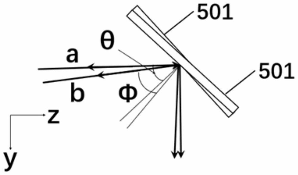
technical field [0001] The invention relates to a narrow line width external cavity semiconductor laser line array based on a diffraction grating array. Background technique [0002] There is inherent thermal stress in the process of bonding the laser line array with the heat sink, so that each light-emitting unit in the line array is not on a straight line and bends. When using the entire diffraction grating external cavity feedback for spectral compression, such as figure 1 As shown, the light-emitting unit a on the optical axis (z-axis) and the off-axis light-emitting unit b are incident on the grating at different angles. When the diffraction grating is a Littrow structure, the center wavelength of the feedback light returning from the original path is different. Different from the central wavelength of the spectrum output by the off-axis light-emitting unit, the overall spectrum of the semiconductor laser line array is the superposition of the spectra of each light-emi...

Claims


Application Information

Patent Timeline
Patent Type & Authority Applications(China)
IPC IPC(8): H01S5/026H01S5/00
CPCH01S5/005H01S5/026H01S5/0267H01S5/0268
Inventor 杨明来
Owner 浙江长芯光电科技有限公司
Learn More