Method for improving ESD failure of protection ring region of planar Schottky product

A product protection and planar technology, applied in the direction of electrical components, semiconductor/solid-state device manufacturing, circuits, etc., can solve problems such as unstable operation and damage of electronic and electrical products

Active Publication Date: 2021-04-09
YANGZHOU YANGJIE ELECTRONIC TECH CO LTD
View PDF6 Cites 0 Cited by
  • Summary
  • Abstract
  • Description
  • Claims
  • Application Information

AI Technical Summary

Problems solved by technology

Static electricity often causes unstable operation...

Method used


Image

  • Method for improving ESD failure of protection ring region of planar Schottky product
  • Method for improving ESD failure of protection ring region of planar Schottky product
  • Method for improving ESD failure of protection ring region of planar Schottky product

Examples


Embodiment Construction

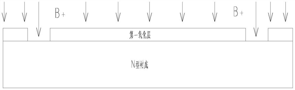
[0030] Shown below with reference to Fig. 1-6; A kind of method that improves planar Schottky product protection ring area ESD failure, is characterized in that, comprises the following steps:

[0031] 1) Grow the first oxide layer (sio) on the surface of the N-type substrate (wafer) 2 ),Such as figure 1 shown;

[0032] 2) Perform a photolithography process on the first oxide layer (the photolithography process includes glue coating, exposure and development; the purpose of the photolithography process is to transfer the pattern from the photolithography plate to the photoresist to the oxide layer, which belongs to the prior art), And through the wet process in the prior art, a ring-shaped groove is etched on the first oxide layer (the purpose of etching the ring-shaped groove is to reserve a region for implanting doping), such as figure 2 shown;

[0033] 3) Remove the surface photoresist and implant B elements; change the charge distribution in the annular groove area, an...


PUM


Abstract

The invention discloses a method for improving an ESD failure of a protection ring region of a planar Schottky product. The method relates to a semiconductor diffusion process. According to the method for improving the ESD failure of the protection ring region of the planar Schottky product, the electric field intensity of the protection ring region is dispersed, so that the anti-static capability of the protection ring region is improved. By increasing the junction depth of a protection ring and increasing the curvature radius of a depletion layer at the edge of the protection ring, the electric field intensity of the ring region is dispersed, so that the antistatic capacity of the protection ring region is improved, and the purpose of increasing the junction depth of the protection ring is achieved by optimizing the oxidation time and temperature of high-temperature diffusion. The method has the advantages of improving the anti-static capability of the protection ring region and the like.

Description

technical field [0001] The invention relates to a semiconductor diffusion process, in particular to a method for improving ESD failure in the protection ring area of ​​planar Schottky products. Background technique [0002] ESD (Electro-Static discharge) means "electrostatic discharge". An object has accumulated a large amount of static (positive or negative) charges, and the object is electrostatically charged to the outside. When the charged object is in contact with or close to other objects, the static charge on the surface will suddenly discharge the static electricity to other objects. Static electricity often causes unstable operation or even damage of electronic and electrical products. ESD (Electrostatic Discharge) discharge current is too large, generating high heat energy, which is easy to break down the internal circuits in electronic appliances. [0003] For planar Schottky products, the electric field intensity in the drift region is linearly distributed, the...

Claims


Application Information

Patent Timeline
IPC IPC(8): H01L21/225H01L21/265H01L21/311H01L21/329H01L21/266
CPCH01L21/2256H01L21/31111H01L21/31144H01L21/26513H01L29/66143H01L21/266
Inventor 陈维伟赵晓非杨亚峰杨正铭陆益王毅
Owner YANGZHOU YANGJIE ELECTRONIC TECH CO LTD
Why Eureka
Try Eureka