Gallium nitride single crystal based on ScAlMgO4 substrate, and preparation method thereof

A gallium nitride single crystal and substrate technology, applied in the field of semiconductors, can solve the problems of complex stripping and dislocation reduction process, high dislocation of gallium nitride crystal, high production cost, etc., to achieve reduced production cost, large radius of curvature , the effect of reducing dislocation

Inactive Publication Date: 2020-09-01
WUXI WUYUE SEMICON CO LTD
View PDF5 Cites 4 Cited by
  • Summary
  • Abstract
  • Description
  • Claims
  • Application Information

AI Technical Summary

Problems solved by technology

[0005] However, this method has disadvantages: the sapphire-based HVPE adopts a heterogeneous material with a lattice mismatch constant of -13.9%, and the dislocation ratio of the grown gallium nitride crystal is relatively high, and at the same time, the stress curvature radius is below 10 meters. The expansion to 4 inches is limited. At the same time, the stripping and dislocation reduction process is complicated, resulting in low yield. In the end, only the single-chip method can be used, which makes the production cost too high.

Method used


Image

  • Gallium nitride single crystal based on ScAlMgO4 substrate, and preparation method thereof

Examples


Embodiment 1

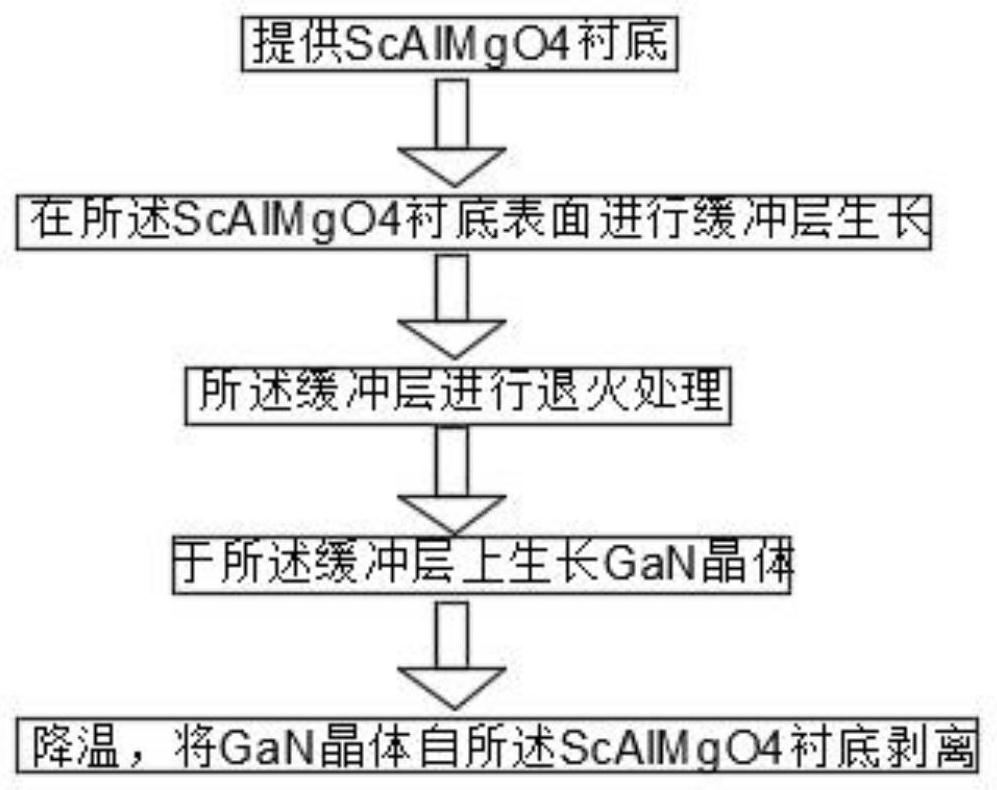
[0029] see figure 1 , the present invention provides a ScAlMgO-based 4 A method for preparing a gallium nitride single crystal of a substrate, comprising the steps of:

[0030] (1) Provide ScAlMgO 4 Substrate;

[0031] (2) In the ScAlMgO 4 Growth of a buffer layer on the surface of the substrate;

[0032] (3) The buffer layer is annealed;

[0033] (4) growing GaN crystals on the buffer layer;

[0034] (5) cooling, the GaN crystal from the ScAlMgO 4 Substrate peeled off.

[0035] see figure 1 and step (1), providing ScAlMgO 4 Substrate 100.

[0036] As a preferred setting of this embodiment, the ScAlMgO 4 The substrate is a circle or a regular polygon; more preferably, the ScAlMgO 4 The substrate is circular or regular hexagonal.

[0037] As a preferred setting of this embodiment, the ScAlMgO 4 Has high crystal quality, its (001) XRDFWHM is generally less than 20 arcsec, preferably less than 10 arcsec; the ScAlMgO 4 The substrate has an atomic layer surface and i...

Embodiment 2

[0046] The present invention also provides a ScAlMgO-based 4 GaN single crystal preparation method of the substrate, described in this example based on ScAlMgO 4 The preparation method of gallium nitride single crystal of the substrate is roughly the same as the preparation method described in other embodiments, the difference is that the growth of the buffer layer described in step (2) of embodiment 2 adopts the MOCVD method to grow the thin film template with a thickness of 1-10um, Its (102)XRDFWHM is less than 320 arcsec, preferably less than 240 arcsec. The MOCVD method is well known to those skilled in the art, and its principle will not be repeated here.

[0047] In step (3), in-situ annealing is performed in an MOCVD furnace, that is, after the low-temperature growth is completed, the temperature is raised to 1000° C. for annealing treatment.

Embodiment 3

[0049] The present invention also provides a ScAlMgO-based 4 GaN single crystal preparation method of the substrate, described in this example based on ScAlMgO 4 The preparation method of the gallium nitride single crystal of the substrate is roughly the same as that described in other embodiments, the difference is that the buffer layer growth in step (2) in this embodiment adopts the high temperature AlNHVPE method. Preferably, under the HVPE process conditions, the temperature is set at 1000-1600°C; more preferably, the temperature is set at 1200-1600°C; more preferably, the temperature is set at 1500-1600°C, and the thickness is 50-3000nm.

[0050] As a preferred setting of Example 3 of the present invention, the buffer layer prepared by the AlNHVPE method may not be annealed, or may be annealed at a high temperature of 1600-1700° C. in a reducing environment in step (3).


PUM

PropertyMeasurementUnit
surface roughnessaaaaaaaaaa
thicknessaaaaaaaaaa
thicknessaaaaaaaaaa

Abstract

The invention provides a preparation method of a gallium nitride single crystal based on an ScAlMgO4 substrate. The preparation method comprises the following steps: (1) providing the ScAlMgO4 substrate; (2) growing a buffer layer on the surface of the ScAlMgO4 substrate; (3) carrying out annealing treatment on the buffer layer; (4) growing a GaN crystal on the buffer layer; and (5) cooling to make the GaN crystal automatically stripped from the ScAlMgO4 substrate. A complex process of depositing GaN and carrying out pretreatment to manufacture a mask or a separation layer by MOCVD is not needed, so that the production cost is effectively reduced; compared with a traditional substrate such as sapphire, the GaN substrate has higher quality and larger curvature radius, and the problem that OFFCUT is uneven when GaN of 4 inches or above grows is solved; and finally, the continuous growth of the crystal bar with the thickness of 5 mm or above can be realized, and the cost is further reduced.

Description

technical field [0001] The invention relates to the field of semiconductor technology, in particular to a ScAlMgO-based 4 Gallium nitride single crystal of the substrate and its preparation method. Background technique [0002] GaN is a typical representative of the third-generation wide-bandgap semiconductors. It has been widely used in semiconductor lighting, microwave power devices, and power electronic devices, showing great application prospects. The most ideal substrate for gallium nitride growth is naturally gallium nitride single crystal material. Such homoepitaxial (that is, the epitaxial layer and the substrate are the same material) can greatly improve the crystal quality of the epitaxial film and reduce the dislocation density. , Improve the working life of the device, improve the luminous efficiency, and increase the working current density of the device. However, gallium nitride single crystal growth is difficult and expensive, and large-scale homoepitaxial g...

Claims


Application Information

Patent Timeline
Patent Type & Authority Applications(China)
IPC IPC(8): C30B29/40C30B25/18C23C14/06C23C14/34C23C14/58C23C16/34C23C16/56
CPCC30B29/406C30B25/183C23C14/0617C23C14/34C23C14/5806C23C16/303C23C16/56C30B25/16
Inventor 张海涛许彬庞博刘良宏
Owner WUXI WUYUE SEMICON CO LTD
Why Eureka
Try Eureka