Single photon avalanche photodiode and manufacturing method thereof

A photodiode and single-photon avalanche technology, which is applied in the field of single-photon detection, can solve the problems of premature edge breakdown, low maximum bias voltage, and affecting the photodetection of avalanche photodiodes.

Active Publication Date: 2016-10-26
量敏传感技术(上海)有限公司
View PDF5 Cites 4 Cited by
  • Summary
  • Abstract
  • Description
  • Claims
  • Application Information

AI Technical Summary

Problems solved by technology

[0003] At present, guard rings of other structures are used to avoid the edge effect of avalanche photodiodes and prevent premature breakdown of the edges, but the maximum bias voltage that the guard rings of other structures can withstand is too low. Under the condition, premature edge breakdown is prone to occur
For some single-photon detection systems with excessive reverse bias voltage swing, the edge effect will occur at the edge under high bias voltage, which will affect the normal photodetection of the avalanche photodiode

Method used


Image

  • Single photon avalanche photodiode and manufacturing method thereof

Examples


Embodiment Construction

[0017] The present invention will be further described below in conjunction with the drawings.

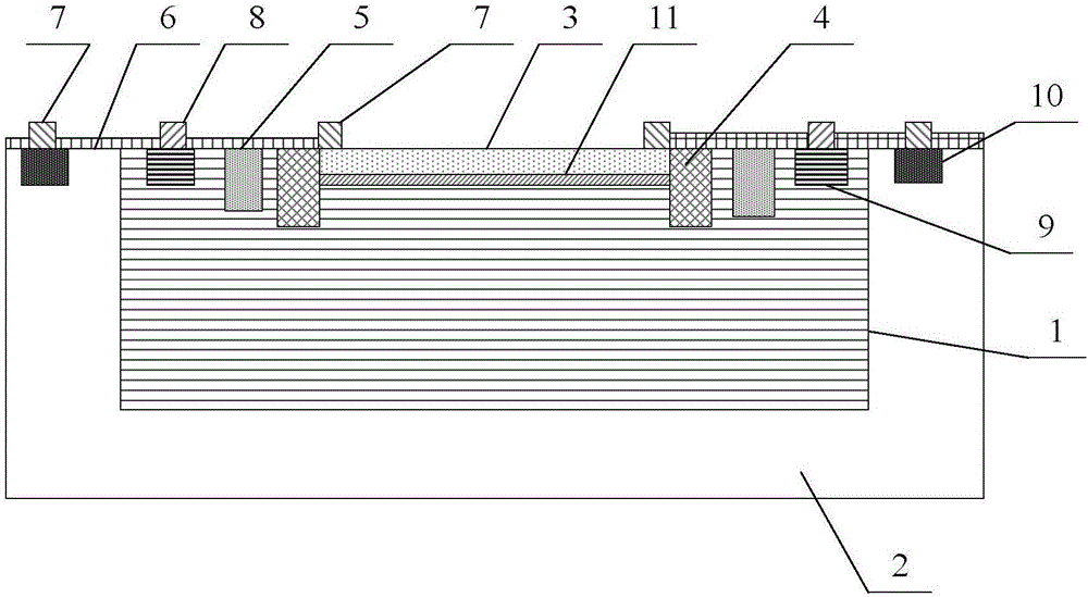
[0018] Reference figure 1 , Single-photon avalanche photodiode, including deep n-well layer 1, p-substrate layer 2, first p+ type semiconductor layer 3, p-well layer 4, p-type semiconductor layer 5, silicon dioxide layer 6, anode electrode 7 And cathode electrode 8, n+ type semiconductor layer 9 and second p+ type semiconductor layer 10; p-well layer 4, p- type semiconductor layer 5, anode electrode 7, cathode electrode 8, n+ type semiconductor layer 9 and second p+ type The semiconductor layer 10 has a circular ring shape. The deep n-well layer 1 is located in the central doped region of the p-substrate layer 2; the p-well layer 4, the p-type semiconductor layer 5 and the n+-type semiconductor layer 9 are all located in the outer end surface doped region of the deep n-well layer, and p The-type semiconductor layer 5 is located between the outer circumference of the p- well layer an...


PUM


Abstract

The invention discloses a single photon avalanche photodiode and a manufacturing method thereof. A maximum bias voltage borne by a protection ring of an existing single photon avalanche photodiode is too low. The manufacturing method of the single photon avalanche photodiode comprises the following steps that a silicon substrate is uniformly doped with a p- substrate and a center of the p- substrate is doped with a deep n trap layer; an outer end of the deep n trap layer is doped with a first p+ type semiconductor layer and an outer side of the first p+ type semiconductor layer is doped with a p- trap layer; a periphery of the p- trap layer is doped with a p- type semiconductor layer; a periphery of the p- type semiconductor layer is doped with a n+ type semiconductor layer and a periphery of the n+ type semiconductor layer is doped with a second p+ type semiconductor layer; outer ends of the first p+ type semiconductor layer and the second p+ type semiconductor layer are provided with anode electrodes and an outer end of the n+ type semiconductor layer is provided with a cathode electrode. In the invention, a maximum reverse bias voltage borne by the avalanche photodiode can reach 30.51V.

Description

Technical field [0001] The invention belongs to the technical field of single-photon detection, and specifically relates to a single-photon avalanche photodiode and a manufacturing method thereof. Background technique [0002] Single photon detection technology is a very low light detection sensor technology, which has a wide range of applications in the fields of bioluminescence, quantum communication, atmospheric pollution detection, radiation detection, astronomical research, and high-sensitivity sensors. The photoreceiving devices used in the single-photon detection technology mainly include photomultiplier tubes (PTM) and single-photon avalanche diodes (APD). In a single-photon detection system using a single-photon avalanche photodiode, the edge effect is a key factor that affects the single-photon detection of the avalanche photodiode, and the guard ring is an important means to avoid the edge effect. Therefore, how to avoid the edge effect of the avalanche photodiode and...

Claims


Application Information

Patent Timeline
Patent Type & Authority Applications(China)
IPC IPC(8): H01L31/107H01L31/18
CPCH01L31/107H01L31/18
Inventor 王伟张钰卫振奇
Owner 量敏传感技术(上海)有限公司
Why Eureka
Try Eureka