High-speed photoelectronic device based on polar J-TMDs/beta-Ga2O3 heterojunction and preparation method thereof

An optoelectronic device, -ga2o3 technology, applied in electrical components, semiconductor devices, circuits, etc., can solve problems such as difficult to meet actual needs, achieve the effect of improving fine patterning, achieve precise control, and improve separation and transmission.

Inactive Publication Date: 2021-04-09
XIDIAN UNIV
View PDF5 Cites 4 Cited by
  • Summary
  • Abstract
  • Description
  • Claims
  • Application Information

AI Technical Summary

Problems solved by technology

In 2009, Japanese scholar R Sukuki et al. published the article "Vertical solar-blind deep-ultraviolet schottky photodetectors based on β-Ga 2 o 3 In Substrates, it is proposed that in single crystal β-Ga 2 o 3 Preparation of Au / β-Ga on Substrate 2 o 3 Photodetectors with Shockley contacts, such as figure 1 As shown in (a), the results show that the maximum photoresponsivity of the annealed sample can reach 10 3 A / W, but its light response time is only about 9ms, which is difficult to meet actual needs
In 2013, Nakagomi et al. published the article "Deep ultraviolet photodiodes based on β-Ga 2 o 3 / SiCheterojunction" proposed to grow about 200nm β-Ga on the P-type 6H-SiC substrate 2 o 3 thin film, formed with β-Ga 2 o 3 / SiC heterojunction photodetectors, such as figure 1 As shown in (b), although the detector exhibits good rectification characteristics and good photoresponsivity, the response time of the detector is still on the order of milliseconds, which is much higher than that of mature silicon-based photodetectors in nanoseconds class response time

Method used


Image

  • High-speed photoelectronic device based on polar J-TMDs/beta-Ga2O3 heterojunction and preparation method thereof
  • High-speed photoelectronic device based on polar J-TMDs/beta-Ga2O3 heterojunction and preparation method thereof
  • High-speed photoelectronic device based on polar J-TMDs/beta-Ga2O3 heterojunction and preparation method thereof

Examples


Embodiment 1

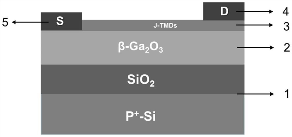
[0063] Embodiment 1: Preparation of SiO 2 The thickness of the gate dielectric layer is 150nm substrate; β-Ga 2 o 3 The surface area of ​​the layer is 1 cm 2 , thickness is 60nm; TMDs layer is MoS 2 Materials, the polar J-TMDs layer is a two-dimensional Janus-MoSSe material with a thickness of 1nm; the source and drain electrodes are made of Al metal with a thickness of 100nm based on polar J-TMDs / β-Ga 2 o 3 High-speed optoelectronic devices with heterojunctions.

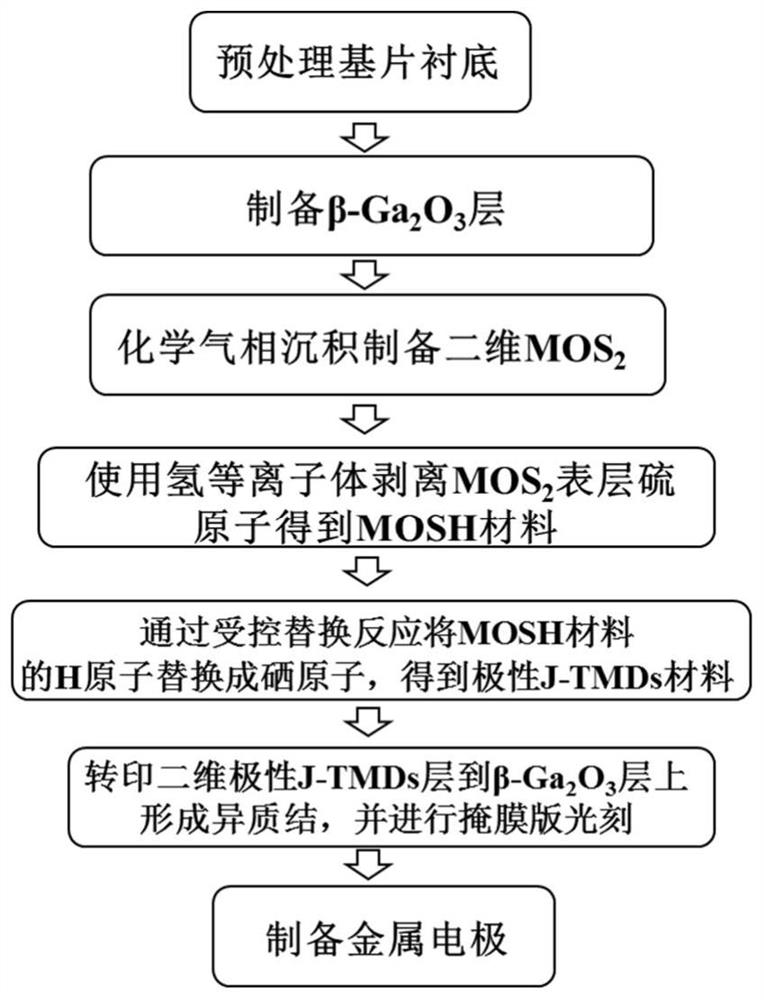
[0064] refer to image 3 , the implementation steps of this example are as follows:

[0065] Step 1: Pretreatment of SiO 2 / Si substrate substrate.

[0066] 1.1) Choose SiO2 2 Layer thickness 150nm, area 1cm 2 SiO 2 / Si substrate, place the substrate in a beaker and ultrasonically clean it in an acetone solution for 10-20 minutes, then place the substrate in an ethanol solution and clean it for 10-20 minutes to remove residual acetone, and finally clean it ultrasonically in deionized water 5min;

[0067...

Embodiment 2

[0094] Embodiment 2: Preparation of SiO 2 The thickness of the gate dielectric layer is 200nm substrate; β-Ga 2 o 3 The surface area of ​​the layer is 1 cm 2 , with a thickness of 120nm; the TMDs layer is MoSe 2 Materials, the polar J-TMDs layer is a two-dimensional Janus-MoSSe material with a thickness of 1nm; the source and drain electrodes are made of Au metal with a thickness of 120nm based on polar J-TMDs / β-Ga 2 o 3 High-speed optoelectronic devices with heterojunctions.

[0095] refer to Figure 4 , the implementation steps of this example are as follows:

[0096] Step 1: Pretreatment of SiO 2 / Si substrate substrate.

[0097] 1a) Choose SiO2 2 Layer thickness 200nm, area 1cm 2 SiO 2 / Si substrate, place the substrate in a beaker and ultrasonically clean it in an acetone solution for 10-20 minutes, then place the substrate in an ethanol solution and clean it for 10-20 minutes to remove residual acetone, and finally clean it ultrasonically in deionized water 5...

Embodiment 3

[0115] Embodiment 3: Preparation of SiO 2 The thickness of the gate dielectric layer is 300nm substrate; β-Ga 2 o 3 The surface area of ​​the layer is 1 cm 2 , thickness is 180nm; TMDs layer is MoS 2 Materials, the polar J-TMDs layer is a two-dimensional Janus-MoSSe material with a thickness of 1nm; the source and drain electrodes are made of Ti / Au alloy with a thickness of 150nm based on polar J-TMDs / β-Ga 2 o 3 High-speed optoelectronic devices with heterojunctions.

[0116] refer to image 3 , the implementation steps of this example are as follows:

[0117] Step A: Pretreatment of SiO 2 / Si substrate substrate.

[0118] Choose SiO2 2 Layer thickness 300nm, area 1cm 2 SiO 2 / Si substrate, place the substrate in a beaker and ultrasonically clean it in acetone solution for 10-20 minutes; then place the substrate in an ethanol solution and clean it for 10-20 minutes to remove residual acetone, and then ultrasonically clean it in deionized water 5min, and dry the cle...


PUM

PropertyMeasurementUnit
thicknessaaaaaaaaaa
thicknessaaaaaaaaaa
thicknessaaaaaaaaaa

Abstract

The invention discloses a high-speed photoelectronic device based on a polar J-TMDs / beta-Ga2O3 heterojunction and a preparation method thereof. The problem that an existing beta-Ga2O3-based photoelectronic device is low in response speed is mainly solved. The high-speed photoelectronic device comprises a substrate (1), a beta-Ga2O3 light absorption layer (2) and metal source and drain electrodes (4 and 5), the substrate adopts an SiO2 / Si substrate, SiO2 is used as a gate dielectric material, and Si is used as a gate electrode at the bottom; a polar J-TMDs layer is arranged at the upper part of the beta-Ga2O3 light absorption layer and is used for forming a heterojunction with the light absorption layer to inhibit exciton recombination, so that charges are quickly transferred at the interface of the heterojunction; and the metal source electrode is located at one end of the beta-Ga2O3 layer, and the metal drain electrode is located at one end, opposite to the metal source electrode, of the polar J-TMDs layer. According to the invention, the transmission performance at the interface is improved, the response speed of the device is improved, and the method can be used for preparing a high-performance photoelectric detector.

Description

technical field [0001] The invention belongs to the technical field of semiconductor devices, and further relates to a high-speed optoelectronic device, which is applied to the preparation of high-performance photodetectors. Background technique [0002] Ga 2 o 3 The material is a transparent oxide semiconductor material. As an important member of wide bandgap semiconductor materials, it benefits from the large size Ga 2 o 3 The breakthrough in single crystal preparation technology has become a major research hotspot in the field of semiconductors. Ga 2 o 3 The material has 5 isomers, namely α, β, γ, ε and δ, among which β-Ga 2 o 3 The material is the most stable crystalline structure. β-Ga 2 o 3 It has a very large bandgap width, between 4.2 and 4.9eV, and the absorption wavelength range corresponding to the bandgap range is 253nm to 295nm, extending to the deep ultraviolet region, and has a transmittance of more than 80% for ultraviolet light. The absorbing mate...

Claims


Application Information

Patent Timeline
Patent Type & Authority Applications(China)
IPC IPC(8): H01L31/0352H01L31/0328H01L31/032H01L31/0296H01L31/18
CPCH01L31/035272H01L31/0296H01L31/032H01L31/0321H01L31/0328H01L31/1876Y02P70/50
Inventor 苏杰常晶晶朱小强袁海东林珍华郝跃
Owner XIDIAN UNIV
Why Eureka
Try Eureka