GaN-based HEMT low-temperature gold-free ohmic contact electrode and preparation method thereof

A technology of ohmic contact electrodes and ohmic contact, which is applied in the manufacture of circuits, electrical components, semiconductors/solid-state devices, etc., can solve problems such as limiting use, affecting device dynamic performance, and increasing material square resistance, so as to promote ohmic contact and improve Effects of free carrier concentration and lower annealing temperature

Pending Publication Date: 2021-04-16
ZHONGSHAN INST OF MODERN IND TECH SOUTH CHINA UNIV OF TECH +1
View PDF0 Cites 4 Cited by
  • Summary
  • Abstract
  • Description
  • Claims
  • Application Information

AI Technical Summary

Problems solved by technology

However, on the one hand, high-temperature annealing will introduce high-density deep energy levels/surface states on the surface of AlGaN, thereby affecting the

Method used


Image

  • GaN-based HEMT low-temperature gold-free ohmic contact electrode and preparation method thereof
  • GaN-based HEMT low-temperature gold-free ohmic contact electrode and preparation method thereof
  • GaN-based HEMT low-temperature gold-free ohmic contact electrode and preparation method thereof

Examples


Embodiment 1

[0043] The preparation method of the GaN-based HEMT low-temperature gold-free ohmic contact of this embodiment includes the following steps:

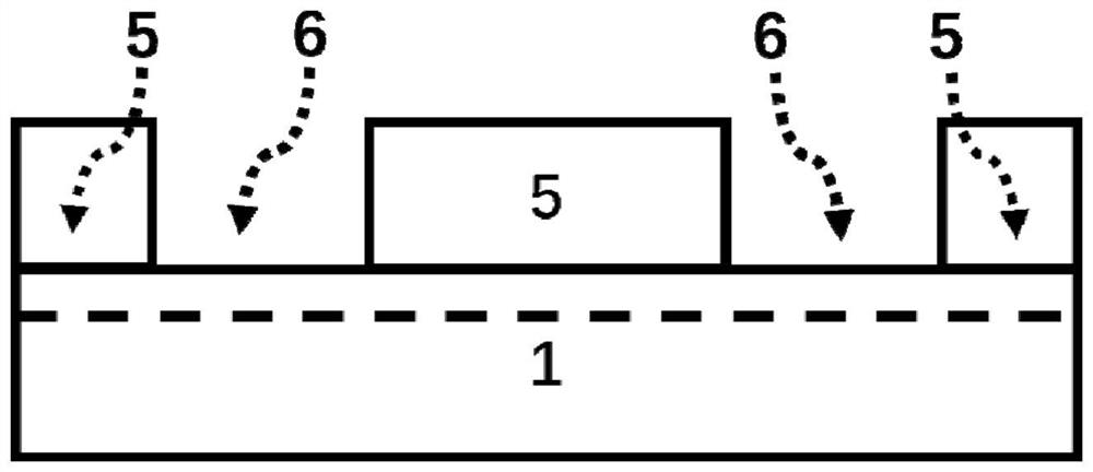
[0044] (1) Using photolithography technology to define source and drain etching pattern areas on the GaN-based epitaxial layer;

[0045] (2) Using ICP etching technology, the AlGaN barrier layer is completely etched away, and etched to the GaN channel layer (the dotted line in the figure refers to the 2DEG channel, and the GaN channel layer below it) down to 10nm , the etching inclination angle is 50°;

[0046] (3) On the basis of retaining the photoresist, use an acid-base solution to clean the source-drain etching pattern obtained in step (2);

[0047] (4) Remove the photoresist in step (3), and after cleaning, put the obtained GaN-based epitaxial layer into a rapid thermal annealing system for surface oxidation treatment to remove the exposed AlGaN / GaN heterojunction sidewall after etching Treat with the GaN channel layer, the anne...

Embodiment 2

[0053] The preparation method of the GaN-based HEMT low-temperature gold-free ohmic contact of this embodiment includes the following steps:

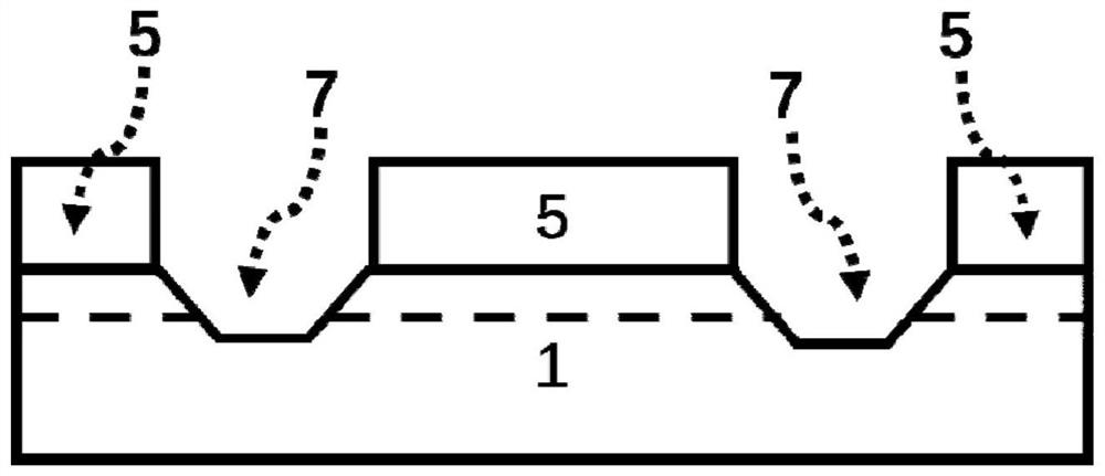
[0054] (1) Using photolithography technology to define source and drain etching pattern areas on the GaN-based epitaxial layer;

[0055] (2) Using ICP etching technology, the AlGaN barrier layer is completely removed, and etched to 20nm below the GaN channel layer, with an etching inclination angle of 40°;

[0056] (3) cleaning the source-drain etching pattern obtained in step (2) by using an acid-base solution;

[0057] (4) Remove the photoresist in step (3), and after cleaning, put the obtained GaN-based epitaxial layer into a rapid thermal annealing system for surface oxidation treatment to remove the exposed AlGaN / GaN heterojunction sidewall after etching Treat with the GaN channel layer, the annealing temperature is 350°C, the annealing time is 20min, and the atmosphere is high-purity oxygen;

[0058] (5) Using photolithography t...

Embodiment 3

[0063] The preparation method of the GaN-based HEMT low-temperature gold-free ohmic contact of this embodiment includes the following steps:

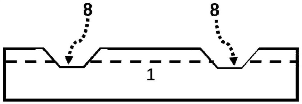
[0064] (1) Using photolithography technology to define source and drain etching pattern areas on the GaN-based epitaxial layer;

[0065] (2) Using ICP etching technology, the AlGaN barrier layer is completely removed, and etched to 50nm below the GaN channel layer, and the etching inclination angle is 20°;

[0066] (3) cleaning the source-drain etching pattern obtained in step (2) by using an acid-base solution;

[0067] (4) Remove the photoresist in step (3), and after cleaning, carry out oxygen plasma treatment on the GaN-based epitaxial layer to treat the exposed AlGaN / GaN heterojunction sidewall and GaN channel layer after etching. Treatment, the oxygen flow rate is 60sccm, the power is 250W, and the time is 200s;

[0068] (5) Using photolithography technology, define a source-drain ohmic contact pattern area for the GaN-based epi...


PUM

PropertyMeasurementUnit
Thicknessaaaaaaaaaa
Thicknessaaaaaaaaaa
Thicknessaaaaaaaaaa

Abstract

The invention discloses a GaN-based HEMT low-temperature gold-free ohmic contact electrode. The GaN-based HEMT low-temperature gold-free ohmic contact electrode comprises a GaN-based HEMT epitaxial layer, wherein a GaN channel layer is arranged in the GaN-based HEMT epitaxial layer. The electrode comprises a first metal layer Ti, a second metal layer Al and a third metal layer TiW which are sequentially arranged on the upper surface of the GaN-based HEMT epitaxial layer from bottom to top, or a first metal layer Ti, a second metal layer Al, a third metal layer Ti and a fourth metal layer TiW which are sequentially arranged from bottom to top. The invention also correspondingly discloses a preparation method of the electrode. According to the invention, the annealing temperature of GaN-based HEMT ohmic contact is effectively reduced, 2DEG leakage caused by overall etching of an AlGaN barrier layer and current reduction during ohmic contact forming are improved, ohmic contact forming difficulty is reduced, and the appearance and edge of an ohmic contact surface after low-temperature alloy annealing are smoother. Meanwhile, the manufacturing cost of a GaN-based HEMT device can be reduced.

Description

technical field [0001] The invention relates to a semiconductor device, in particular to a GaN-based HEMT low-temperature gold-free ohmic contact electrode and a preparation method thereof. Background technique [0002] GaN-based high electron mobility transistors (HEMTs) have broad application prospects in the fields of high-voltage, high-frequency, high-power semiconductor laser devices and high-performance ultraviolet detectors. However, the production line technology for compound semiconductors is relatively backward, and the cost of process update and operation and maintenance is relatively high, which increases the production cost of GaN-based HEMT devices. Using mature and advanced Si-CMOS process lines to produce HEMT devices can effectively reduce the difficulty of manufacturing HEMT devices and reduce manufacturing costs. The heavy metal Au used in the ohmic and Schottky contact processes of conventional HEMT devices will form deep-level impurities in Si and pollu...

Claims


Application Information

Patent Timeline
IPC IPC(8): H01L29/45H01L21/28H01L29/778H01L21/335
Inventor 王洪李先辉
Owner ZHONGSHAN INST OF MODERN IND TECH SOUTH CHINA UNIV OF TECH
Why Eureka
Try Eureka