Semiconductor structure and forming method thereof

A semiconductor and patterning technology, applied in semiconductor devices, semiconductor/solid-state device manufacturing, electrical components, etc., can solve problems such as semiconductor structure performance needs to be improved

Pending Publication Date: 2021-04-23
SEMICON MFG INT (SHANGHAI) CORP +1
View PDF0 Cites 0 Cited by
  • Summary
  • Abstract
  • Description
  • Claims
  • Application Information

AI Technical Summary

Problems solved by technology

[0004] However, the performance of the semiconductor structure formed by the multiple patterning process in the prior art still needs to be improved

Method used


Image

  • Semiconductor structure and forming method thereof
  • Semiconductor structure and forming method thereof
  • Semiconductor structure and forming method thereof

Examples


Embodiment Construction

[0033] As mentioned in the background, the performance of the semiconductor structure formed by the multiple patterning process in the prior art still needs to be improved.

[0034] The following will describe in detail in conjunction with the accompanying drawings.

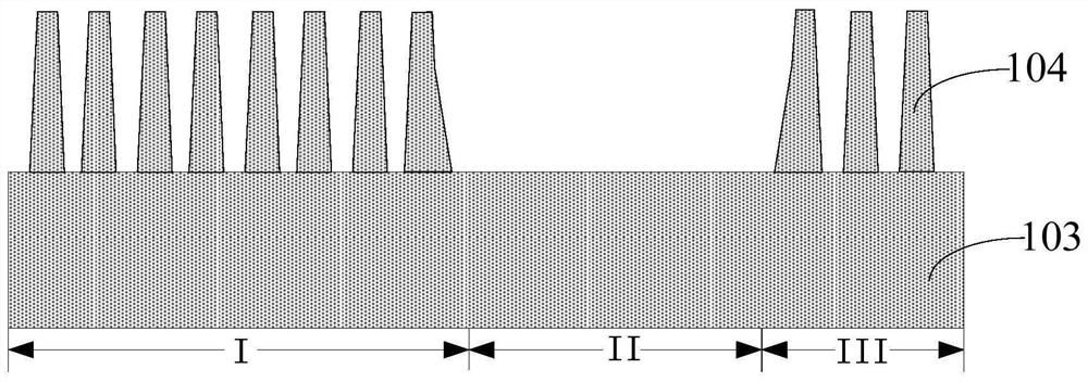
[0035] Figure 1 to Figure 3 It is a structural schematic diagram of each step of an embodiment of a fin forming process.

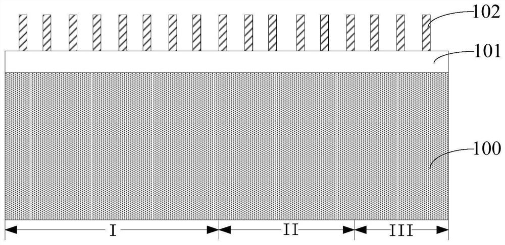
[0036] Please refer to figure 1 , providing an initial substrate 100, the initial substrate 100 includes a first region I, a second region II and a third region III, the first region I, the second region II and the third region III are sequentially adjacent; in the A mask layer 101 is formed on the initial substrate 100; on the mask layer 101, a number of mutually discrete initial patterned structures 102 are formed, and the process of forming the initial patterned structures 102 adopts a multiple patterning process.

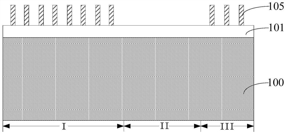
[0037] Please refer to figure 2 , removing the initial patterned str...


PUM


Abstract

The invention discloses a semiconductor structure and a forming method thereof. The method comprises the following steps that: a substrate is provided; a plurality of mutually separated main fin parts and dummy fin parts are formed on the substrate, each dummy fin part comprises a first region and a second region located on the first region, the material of the second region is different from the material of the main fin parts, and the material of the second region is different from the material of the first region; an isolation layer is formed on the substrate, wherein the isolation layer covers a part of the side wall of each main fin portion and the side wall of each first region; and etching is performed to remove the second regions after the isolation layer is formed. The main fin parts and the dummy fin parts which are separated from each other are formed, the consistency of an etching environment in the etching process is ensured, and the size of the bottom of each formed main fin part is prevented from being increased due to the change of the etching environment; and in addition, through etching selectivity of different materials by an etching process, part of the pseudo fin parts are removed, defects caused by a photoetching patterning process are avoided, and the performance of the finally formed semiconductor structure is improved.

Description

technical field [0001] The invention relates to the technical field of semiconductor manufacturing, in particular to a semiconductor structure and a forming method thereof. Background technique [0002] With the continuous progress of semiconductor technology, the process nodes of semiconductor devices are continuously reduced. However, due to the limitation of the precision of the existing photolithography process, the mask pattern formed by the existing photolithography process is difficult to meet the demand for continuous reduction of the feature size of semiconductor devices, which hinders the development of semiconductor technology. [0003] In order to further reduce the size of the semiconductor device on the basis of the existing photolithography process, a multi-patterning process is proposed in the prior art. Among them, the self-aligned quadruple patterning process (SAQP, Self-Aligned Quadruple Pattern) has application prospects because it can form a mask with a...

Claims


Application Information

Patent Timeline
Patent Type & Authority Applications(China)
IPC IPC(8): H01L21/336H01L29/78
CPCH01L29/66606H01L29/66795H01L29/785
Inventor 任飞
Owner SEMICON MFG INT (SHANGHAI) CORP
Why Eureka
Try Eureka