Manufacturing method for SiC MOSFET device and SiC MOSFET device

A manufacturing method and device technology, applied in the fields of semiconductor/solid-state device manufacturing, semiconductor devices, electrical components, etc., can solve the problems of strict polysilicon oxidation process requirements, difficulty in accurately controlling the channel size, and high process difficulty, and achieve a large improvement. The effect of current density output capability, increasing current lateral output path, simple and stable process

Active Publication Date: 2021-04-23
ZHUZHOU CSR TIMES ELECTRIC CO LTD
View PDF8 Cites 4 Cited by
  • Summary
  • Abstract
  • Description
  • Claims
  • Application Information

AI Technical Summary

Problems solved by technology

The self-alignment scheme using oxidized sidewalls requires strict polysilicon oxidation process, and it is difficult to precisely control the channel size...

Method used


Image

  • Manufacturing method for SiC MOSFET device and SiC MOSFET device
  • Manufacturing method for SiC MOSFET device and SiC MOSFET device
  • Manufacturing method for SiC MOSFET device and SiC MOSFET device

Examples


Embodiment 1

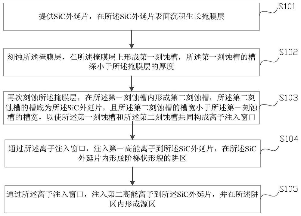
[0050] figure 1 It is a schematic flowchart of a manufacturing method of a SiC MOSFET device shown in an embodiment of the present disclosure. Figure 2-Figure 8 It is a schematic cross-sectional structure formed by related steps of a manufacturing method of a SiC MOSFET device shown in an embodiment of the present disclosure. Below, refer to figure 1 with Figure 2-Figure 8 The detailed steps of an exemplary method of the method for manufacturing a SiC MOSFET device proposed by the embodiments of the present disclosure will be described.

[0051] Such as figure 1 As shown, the SiC MOSFET manufacturing method of this embodiment includes the following steps:

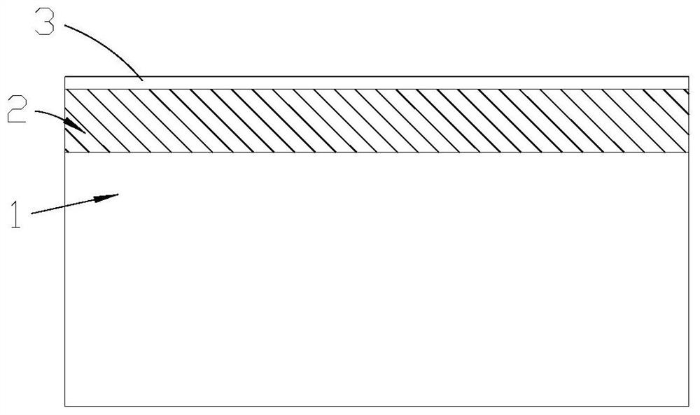
[0052] Step S101 : providing a SiC epitaxial wafer 1 , and depositing a growth mask layer 2 on the surface of the SiC epitaxial wafer 1 .

[0053] In specific implementation, the material for forming the mask layer in the above steps is SiO 2 , SiN, AlN, polysilicon and amorphous silicon.

[0054] Step S102 : etchi...

Embodiment 2

[0082] On the basis of Embodiment 1, this embodiment provides a method using SiO 2 The manufacturing method of N-type SiCMOSFET device as mask layer material, such as figure 1 shown, including the following steps:

[0083] Step S101 : providing an N-type SiC epitaxial wafer 1 , and depositing a growth mask layer 2 on the surface of the N-type SiC epitaxial wafer 1 .

[0084] In specific implementation, the material for forming the mask layer in the above steps is SiO 2 , the thickness of the mask layer is 2um.

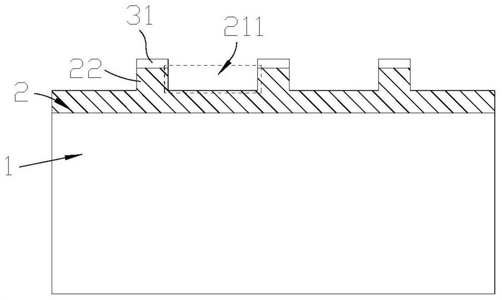
[0085] Step S102 : Etching the mask layer 2 to form a first etching groove 211 on the mask layer. The depth of the first etching groove 211 is smaller than the thickness of the mask layer 2 .

[0086] Specifically, the etching slope angle of the first etching groove 211 in the above step S102 is 90 degrees, and the groove depth is 1.0 um to 1.2 um.

[0087] In the embodiment of the present disclosure, specifically, as figure 2 with image 3 As shown, the above s...

Embodiment 3

[0110] Figure 9 It is a schematic cross-sectional structure diagram of a SiC MOSFET device shown in an embodiment of the present disclosure. Such as Figure 9 As shown, a SiC MOSFET device includes: a SiC epitaxial wafer 1 , a well region 4 with a stepped shape in the SiC epitaxial wafer 1 , and a source region 5 located in the well region 4 .

[0111] It also includes a gate insulating layer 6 located above the SiC epitaxial wafer 1 and between two adjacent source regions 5 , and a polysilicon gate 7 located on the gate insulating layer 6 .

[0112] It also includes an interlayer dielectric layer 8 covering the polysilicon gate, a front metal layer 9 covering the SiC epitaxial wafer 1 and the interlayer dielectric layer 8 , and a back metal layer 10 covering the back of the SiC epitaxial wafer 1 .

[0113] Specifically, the step-shaped well region 4 includes a first well region 41 flush with the surface of the SiC epitaxial wafer 1 and a second well region 42 located below...


PUM

PropertyMeasurementUnit
Thicknessaaaaaaaaaa
Thicknessaaaaaaaaaa
Thicknessaaaaaaaaaa

Abstract

The invention provides a manufacturing method of a SiC MOSFET device and a SiC MOSFET device. The method comprises the following steps of: providing a SiC epitaxial wafer, and depositing and growing a mask layer on the surface of the SiC epitaxial wafer; etching the mask layer, forming a first etching groove in the mask layer; etching the mask layer again, and forming a second etching groove in the first etching groove; injecting first high-energy ions through an ion injection window formed by the first etching groove and the second etching groove to form a stepped well region; and injecting second high-energy ions to form a source region. According to the manufacturing method for the SiC MOSFET device of the invention, the self-alignment process is realized through the ion implantation window with the stepped morphology, the length and position of a channel can be accurately controlled, and the process is simple and stable. Meanwhile, P well regions with the step-shaped morphology are formed, a JFET region between the two P well regions is expanded, so that the current transverse output path of the JFET region is increased, and the large current density output capability of the device is improved.

Description

technical field [0001] The present disclosure relates to the technical field of semiconductor devices, in particular to a method for manufacturing a SiC MOSFET device and the SiC MOSFET device. Background technique [0002] SiC Metal-Oxide-Semiconductor Field-Effect Transistor (SiC MOSFET) has the characteristics of low on-resistance, fast switching speed, and high temperature resistance. It is used in high-voltage frequency conversion, new energy vehicles, rail transit and other fields Has great application advantages. Since SiC material is the only wide bandgap semiconductor material that can directly form SiO through thermal oxidation 2 This advantage simplifies the manufacturing process of SiC MOSFET, which makes SiC MOSFET receive great attention. [0003] At present, in order to improve the performance of SiC MOSFET, the method of shortening the channel length and the area of ​​a single cell in the SiC MOSFET device is generally adopted, so as to increase the number ...

Claims


Application Information

Patent Timeline
IPC IPC(8): H01L29/06H01L29/24H01L21/336H01L29/78H01L21/265
CPCH01L29/78H01L29/66477H01L29/24H01L29/0684H01L21/26506
Inventor 李诚瞻罗烨辉周正东刘芹王志成龚芷玉魏伟戴小平
Owner ZHUZHOU CSR TIMES ELECTRIC CO LTD
Why Eureka
Try Eureka