

Uniform electroplating thickening method for ceramic dielectric filter with blind holes and through holes
A ceramic dielectric and uniform electroplating technology, which is applied in the direction of waveguide devices, circuits, electrical components, etc., can solve problems such as the inability to meet the requirements of ceramic dielectric filters for the thickness consistency of the surface metal layer
- Summary
- Abstract
- Description
- Claims
- Application Information
AI Technical Summary
Problems solved by technology
Method used
Image

Examples
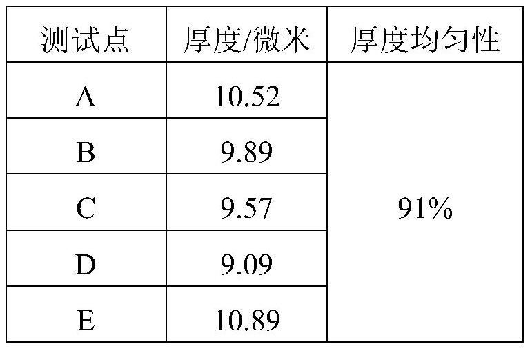
Embodiment 1
[0035] Step (1), preparation of seed layer
[0036] Use anhydrous ethanol to ultrasonically clean the ceramic dielectric filter for 20 minutes, put it in an oven at 300°C for 1 hour, then lower it to room temperature and take it out; then put it in a vacuum chamber, and prepare a seed layer copper layer on the surface of the ceramic dielectric filter by vacuum ion plating , the vacuum chamber is preheated at 200°C, and the vacuum is at 1×10 -3 At Pa, argon gas was introduced and the vacuum was maintained at 7×10 -2 Pa, turn on the arc copper target power supply, set the arc current to 50A, and the coating time depends on the metal deposition rate. In this embodiment, the coating time is 1h, and the thickness of the prepared seed layer copper layer is 500nm.
[0037] Step (2), wrapping the medium diversion film
[0038] The polyimide film (PI film) with good acid and alkali resistance and temperature resistance is used as the dielectric guide film, and the method of laser dri...
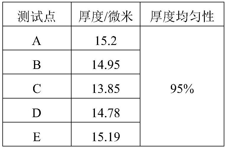
Embodiment 2
[0048] Step (1), preparation of seed layer
[0049] Use anhydrous ethanol to ultrasonically clean the ceramic dielectric filter for 20 minutes, put it in an oven at 300°C for 1 hour, then lower it to room temperature and take it out; then put it in a vacuum chamber, and prepare a seed layer of titanium on the surface of the ceramic dielectric filter by vacuum ion plating Add copper layer, preheat the vacuum chamber at 200°C, vacuum at 1×10 -3 At Pa, argon gas was introduced and the vacuum was maintained at 7×10 -2 Pa, first turn on the arc titanium target power supply, set the arc current to 50A, and the coating time is 20min; then turn off the titanium target power supply, turn on the copper target power supply, set the arc current to 50A, and the coating time is 48min; the thickness of the prepared seed layer is 100nm for the titanium layer , copper layer 400nm.
[0050] Step (2), wrapping the medium diversion film
[0051] The polyimide film (PI film) with good acid and ...
PUM
| Property | Measurement | Unit |
|---|---|---|
| thickness | aaaaa | aaaaa |
| pore size | aaaaa | aaaaa |
| thickness | aaaaa | aaaaa |
Abstract
Description
Claims
Application Information