

Preparation method for silicon nitride film, solar cell with silicon nitride film and preparation method for solar cell
A solar cell and silicon nitride film technology, which is applied in the field of solar cells, can solve the problems of silicon nitride film color chromatic aberration, silicon nitride film growth rate inconsistency, etc., to reduce the level of silicon wafers, improve the growth rate too fast, The effect of improving the pass rate
- Summary
- Abstract
- Description
- Claims
- Application Information
AI Technical Summary
Problems solved by technology
Method used
Image

Examples
Embodiment approach
[0019] According to a typical embodiment of the present invention, the preparation method of the silicon nitride film comprises the following steps: S1, placing the silicon wafer in the tube furnace; S2, feeding nitrogen into the tube furnace, and setting the tube furnace in The temperature is raised to 340° C. to 360° C. under a nitrogen atmosphere, and the temperature is kept constant for 500s to 2000s; and S3 , forming a first silicon nitride film layer and a second silicon nitride film layer sequentially on the silicon wafer by PECVD method.
[0020] In the present invention, the step of constant temperature of the tube furnace is added before setting the first silicon nitride film layer on the silicon wafer. By constant temperature for a period of time, the temperature of the surrounding and the middle of the silicon wafer is consistent, thus ensuring the temperature of the surrounding and the middle of the silicon wafer. The growth rate of the silicon nitride film is cons...
Embodiment 1
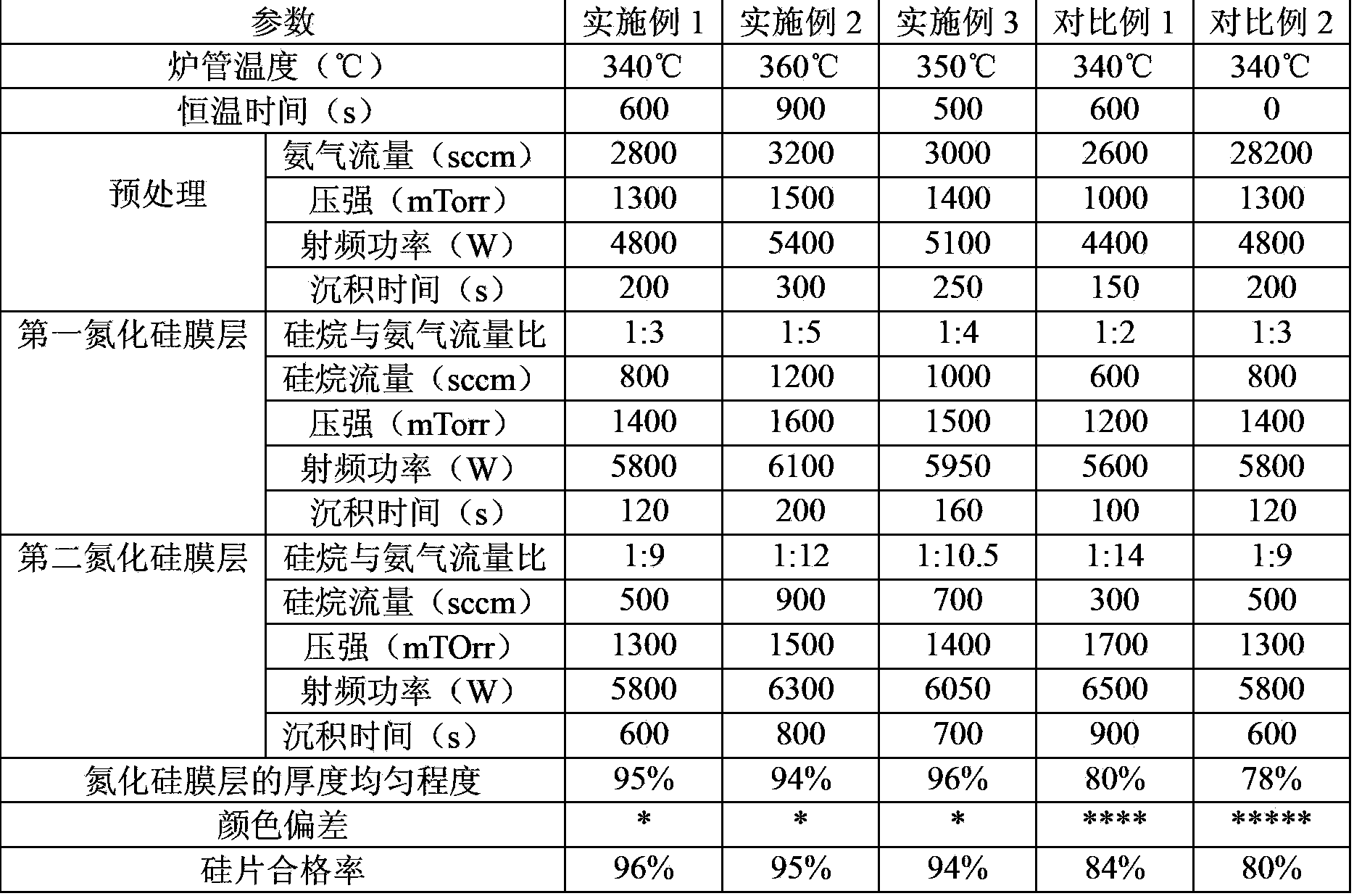
[0033] Introduce nitrogen protection into the quartz tube furnace, push the graphite boat equipped with silicon wafers to be deposited into the quartz tube furnace, raise the temperature to 340°C, feed ammonia gas into the quartz tube furnace with a flow rate of 2800 sccm, and pressurize Under the condition of 1300 mTorr and RF power of 4800W, the PECVD method is used for pretreatment, and the pretreatment time is 200s. After the pretreatment step is completed, the mixed gas is introduced into the quartz tube furnace according to the volume flow ratio of silane and ammonia at 1:3, and the first nitride nitride is deposited by PECVD under the conditions of 1400 mTorr pressure and 5800 W radio frequency power. For the silicon film layer, the deposition time is 120s. According to the volume flow ratio of silane and ammonia gas is 1:9, the mixed gas is introduced into the tube furnace, and the second silicon nitride film layer is deposited by PECVD under the condition of pressure ...
Embodiment 2-3
[0035] The operation steps of Examples 2-3 are the same as those of Example 1, and the specific test conditions such as gas flow rate, pressure, radio frequency power and deposition time are different, see Table 1 for details.
PUM
 Abstract
Description
Claims
Application Information