
Composite substrate, composite film and preparation method thereof, and radio frequency filter

A composite substrate and composite film technology, applied in semiconductor devices, electrical components, circuits, etc., can solve the problems of reducing the service life of radio frequency filters, increasing the debonding of radio frequency filters, and falling off functional films, so as to reduce the risk of debonding and reduce the risk of debonding. The effect of avoiding falling off and prolonging the service life

Active Publication Date: 2021-04-30
JINAN JINGZHENG ELECTRONICS
View PDF7 Cites 0 Cited by
  • Summary
  • Abstract
  • Description
  • Claims
  • Application Information

AI Technical Summary

Problems solved by technology

[0005] The application provides a composite substrate, a composite film and its preparation method, and a radio frequency filter to solve the problem that in the prior art, the composite film is easily debonded at the interface with poor bonding force during the cutting process, causing the functional film to fall off and affecting The use of this area; in addition, the weaker binding force will also increase the risk of debonding during the use of RF filters and reduce the service life of RF filters

Method used


Image

  • Composite substrate, composite film and preparation method thereof, and radio frequency filter
  • Composite substrate, composite film and preparation method thereof, and radio frequency filter
  • Composite substrate, composite film and preparation method thereof, and radio frequency filter

Examples


preparation example Construction

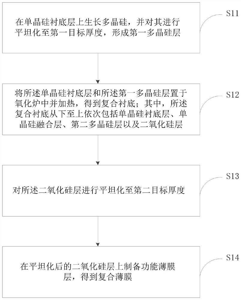
[0051] Specifically, such as image 3 Shown, preparation method comprises the following steps:

[0052] Step S11, growing polysilicon on the single crystal silicon substrate layer 110, and planarizing it to a first target thickness to form a first polysilicon layer 170;

[0053] Optionally, in this step, the monocrystalline silicon substrate layer 110 is injected with gas SiH under the conditions of a temperature greater than or equal to 580° C. and less than or equal to 650° C., and a pressure greater than or equal to 0.1 Torr and less than or equal to 0.4 Torr by using LPCD. 4 , growing polysilicon with a thickness of 1.8 μm; mechanically polishing the polysilicon to 1.4 μm to obtain a first polysilicon layer 170 .

[0054] In step S12, the single crystal silicon substrate layer 110 and the first polycrystalline silicon layer 170 are placed in an oxidation furnace and heated to obtain a composite substrate; wherein the composite substrate includes the single crystal silicon...

Embodiment 1

[0068] Embodiment 1 (ion implantation is combined with bonding separation method)

[0069] 1) Prepare the single crystal silicon substrate layer, and use LPCVD to pass the gas SiH into the single crystal silicon substrate layer at a temperature of 580 ° C and a pressure of 0.1 Torr 4 , growing polysilicon with a thickness of 1.8 μm.

[0070] 2) Mechanically polishing the polysilicon in step 1) to 1.4 μm to obtain the first polysilicon layer.

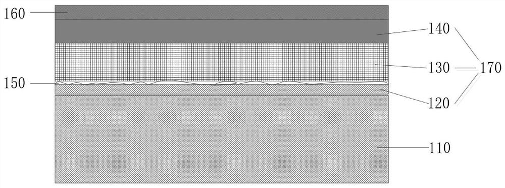
[0071] 3) Place the monocrystalline silicon substrate layer and the first polycrystalline silicon layer in an oxidation furnace at a temperature of 1000° C. and heat for 15 hours to form a silicon dioxide layer with a thickness of 1200 nm, a monocrystalline silicon fusion layer with a thickness of 10 nm and a thickness of 500nm second polysilicon layer.

[0072] 4) Grinding and polishing the silicon dioxide layer in step 3) to 1000 nm.

[0073] 5) Prepare a lithium niobate wafer with the same size as the single crystal silicon substra...

Embodiment 2

[0077] Embodiment 2 (bonding method is combined grinding and polishing method)

[0078] 1) Prepare the single crystal silicon substrate layer, and use LPCVD to pass the gas SiH into the single crystal silicon substrate layer at a temperature of 650 ° C and a pressure of 0.4 Torr 4 , growing polysilicon with a thickness of 1.8 μm.

[0079] 2) Mechanically polishing the polysilicon in step 1) to 1.4 μm to obtain the first polysilicon layer.

[0080] 3) Place the monocrystalline silicon substrate layer and the first polycrystalline silicon layer in an oxidation furnace at a temperature of 900°C and heat for 10 hours to form a silicon dioxide layer with a thickness of 1200 nm, a monocrystalline silicon fusion layer with a thickness of 15 nm, and a thickness of 400nm second polysilicon layer.

[0081] 4) Grinding and polishing the silicon dioxide layer in step 3) to 1000 nm.

[0082] 5) Prepare a lithium niobate wafer of the same size as the single crystal silicon substrate, cle...


PUM

PropertyMeasurementUnit
thicknessaaaaaaaaaa
thicknessaaaaaaaaaa
thicknessaaaaaaaaaa

Abstract

The invention provides a composite substrate, a composite film, a preparation method of the composite film and a radio frequency filter, the composite substrate sequentially comprises a crystalline silicon substrate layer and a first polycrystalline silicon layer from bottom to top, and the first polycrystalline silicon layer comprises a monocrystalline silicon fusion layer, a second polycrystalline silicon layer and a silicon dioxide layer; the monocrystalline silicon fusion layer and the monocrystalline silicon substrate layer are integrally formed; a fusion bulge is formed on one side, close to the second polycrystalline silicon layer, of the monocrystalline silicon fusion layer; and the crystal orientations of the monocrystalline silicon in the monocrystalline silicon substrate layer, the monocrystalline silicon fusion layer and the fusion bulges are the same. By forming the monocrystalline silicon fusion layer between the second polycrystalline silicon layer and the monocrystalline silicon substrate layer, the deposition adhesion of the second polycrystalline silicon layer on the silicon substrate is improved, the risk of debonding of the composite film on an interface with poor bonding force in the cutting process is reduced, the functional film is prevented from falling off, and the utilization rate of the composite film is improved. Meanwhile, the risk of de-bonding in the use process of the radio frequency filter is reduced, and the service life of the radio frequency filter is prolonged.

Description

technical field [0001] The present application relates to the field of semiconductor technology, in particular to a composite substrate, a composite thin film and a preparation method thereof, and a radio frequency filter. Background technique [0002] RF filters are widely used in the transceiver links of wireless communication terminals, allowing signals of specific frequencies or frequency bands to pass through while filtering out unwanted interference or spurious signals. RF filters mainly include surface acoustic wave filter (SAWFilter) and bulk acoustic wave filter (BAW Filter), whose frequency ranges from 800 to 2500MHz. Among them, the energy of the surface acoustic wave in the surface acoustic wave filter is focused on the surface of the substrate, so that the wave propagates without loss on the substrate. By simultaneously controlling the linear expansion coefficient of the substrate and the speed of sound to reduce the frequency temperature coefficient, the electr...

Claims


Application Information

Patent Timeline
Patent Type & Authority Applications(China)
IPC IPC(8): H01L33/02H01L33/00
CPCH01L33/02H01L33/00
Inventor 李洋洋李真宇杨超胡卉刘阿龙连坤
Owner JINAN JINGZHENG ELECTRONICS
Learn More