
A kind of preparation method of composite substrate, composite substrate and composite thin film

A technology of composite substrate and composite film, which is applied in semiconductor/solid-state device manufacturing, semiconductor/solid-state device components, semiconductor devices, etc., can solve the risk of increasing the debonding of radio frequency filters, reduce the service life of radio frequency filters, and functional thin films To reduce the risk of debonding, prolong the service life and avoid falling off

Active Publication Date: 2022-03-15
JINAN JINGZHENG ELECTRONICS
View PDF8 Cites 0 Cited by
  • Summary
  • Abstract
  • Description
  • Claims
  • Application Information

AI Technical Summary

Problems solved by technology

[0005] This application provides a method for preparing a composite substrate, a composite substrate, and a composite film to solve the problem that in the prior art, during the cutting process, the composite film is easily debonded at the interface with poor bonding force, causing the functional film to fall off and affecting this area. In addition, the weak binding force will also increase the risk of debonding during the use of RF filters and reduce the service life of RF filters

Method used


Image

  • A kind of preparation method of composite substrate, composite substrate and composite thin film
  • A kind of preparation method of composite substrate, composite substrate and composite thin film
  • A kind of preparation method of composite substrate, composite substrate and composite thin film

Examples


Embodiment Construction

[0026] The technical solutions in the embodiments of the present application will be clearly and completely described below in conjunction with the accompanying drawings in the embodiments of the present application. Obviously, the described embodiments are only some of the embodiments of the present application, not all of them. Based on the embodiments in this application, all other embodiments obtained by persons of ordinary skill in the art without creative efforts fall within the protection scope of this application.

[0027] As mentioned in the background technology of this application, in the prior art, the volume of the radio frequency filter is relatively small, and the cutting size of the lithium tantalate thin film wafer needs to be smaller. Therefore, the bonding force between the layers of the lithium tantalate thin film wafer is It becomes a key factor in the utilization rate of lithium tantalate film and the yield of devices. If the adhesion of polysilicon depos...


PUM

PropertyMeasurementUnit
thicknessaaaaaaaaaa
lengthaaaaaaaaaa
lengthaaaaaaaaaa

Abstract

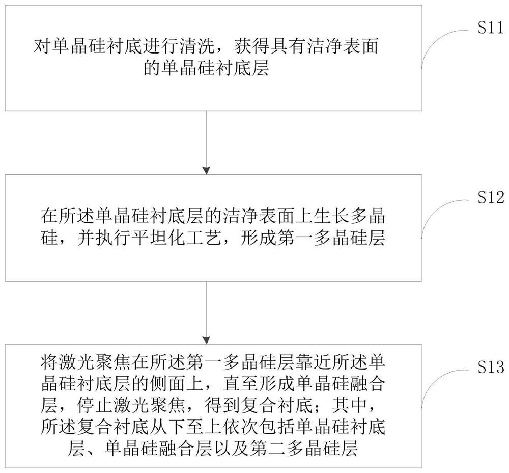
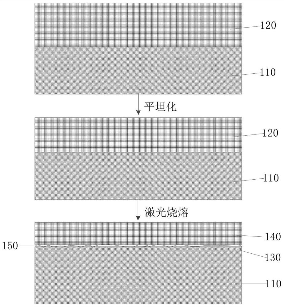
The present application provides a preparation method of a composite substrate, a composite substrate and a composite film, wherein the preparation method of the composite substrate includes: cleaning a single crystal silicon substrate to obtain a single crystal silicon substrate layer with a clean surface; Growing polysilicon on the clean surface of the crystalline silicon substrate layer, and performing a planarization process to form the first polysilicon layer; focusing the laser on the side of the first polysilicon layer close to the monocrystalline silicon substrate layer until the formation of monocrystalline silicon The fusion layer stops laser focusing to obtain a composite substrate; wherein the composite substrate sequentially includes a single crystal silicon substrate layer, a single crystal silicon fusion layer and a second polysilicon layer from bottom to top. Using the aforementioned scheme, by adjusting the power, focal length and position of the laser, the position, distribution and size of the single crystal silicon fusion area can be accurately controlled, so that the target at the target interface can be controlled according to the actual situation of the single crystal silicon substrate layer and the polycrystalline silicon layer. The bonding strength of the area is improved, which improves the adhesion of polysilicon deposited on the silicon substrate.

Description

technical field [0001] The present application relates to the field of semiconductor technology, in particular to a method for preparing a composite substrate, a composite substrate and a composite thin film. Background technique [0002] RF filters are widely used in the transceiver links of wireless communication terminals, allowing signals of specific frequencies or frequency bands to pass through while filtering out unwanted interference or spurious signals. RF filters mainly include surface acoustic wave filter (SAWFilter) and bulk acoustic wave filter (BAW Filter), whose frequency ranges from 800 to 2500MHz. Among them, the energy of the surface acoustic wave in the surface acoustic wave filter is focused on the surface of the substrate, so that the wave propagates without loss on the substrate. By simultaneously controlling the linear expansion coefficient of the substrate and the speed of sound to reduce the frequency temperature coefficient, the electrode generates ...

Claims


Application Information

Patent Timeline
Patent Type & Authority Patents(China)
IPC IPC(8): H01L21/20H01L23/14
CPCH01L21/20H01L23/14
Inventor 李洋洋李真宇杨超胡卉刘阿龙连坤
Owner JINAN JINGZHENG ELECTRONICS
Learn More