Thin-film lithium niobate electrooptical modulator and preparation method thereof

An electro-optic modulator and lithium niobate technology, which is applied in the fields of instruments, optics, nonlinear optics, etc., can solve the problems of high manufacturing process requirements, high difficulty, and high driving voltage

Active Publication Date: 2021-05-07
ZHEJIANG UNIV
View PDF5 Cites 3 Cited by
  • Summary
  • Abstract
  • Description
  • Claims
  • Application Information

AI Technical Summary

Problems solved by technology

[0005] In order to solve the problems existing in the background technology, the present invention proposes a thin-film lithium niobate electro-optic modulator based on an alumina substrate and its preparation method, which effectively solves the problem of high preparation process requirements, great difficulty, and the preparation of thin-film lithium niobate Lithium modulator has high loss, high driving voltage and small bandwidth

Method used


Image

  • Thin-film lithium niobate electrooptical modulator and preparation method thereof
  • Thin-film lithium niobate electrooptical modulator and preparation method thereof
  • Thin-film lithium niobate electrooptical modulator and preparation method thereof

Examples


Embodiment 1

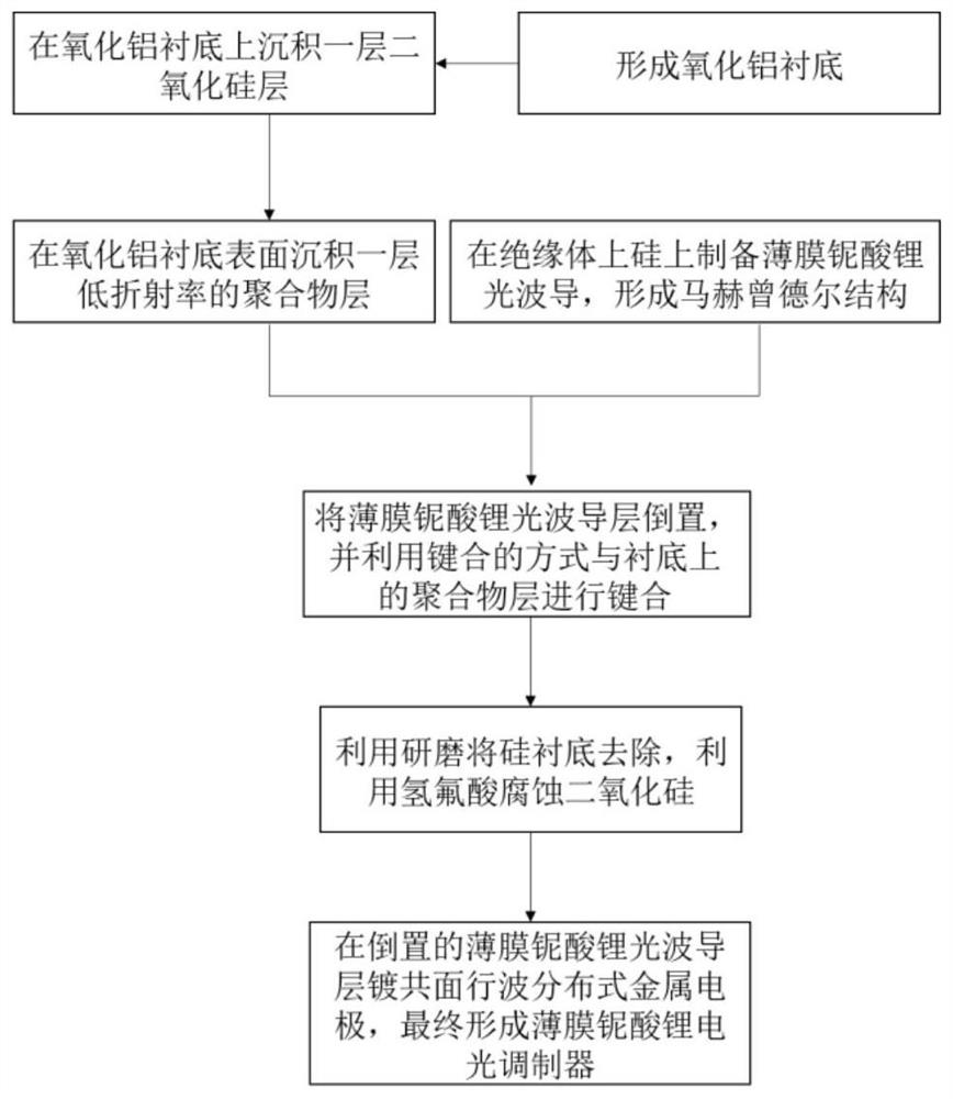
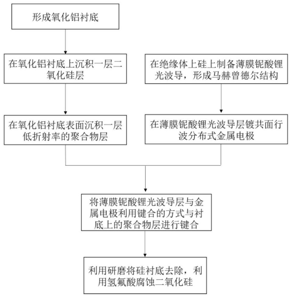
[0066] Such as Figure 8 As shown, this embodiment includes a substrate 1, a buried oxide layer 2, a polymer layer 3 and an optical waveguide layer 4 arranged sequentially from bottom to top, [that is, the buried oxide layer 2 is placed on the substrate 1, and the polymer layer 3 is placed on the On the buried oxide layer 2 , the optical waveguide layer 4 is placed on the polymer layer 3 . 】

[0067] Arrange the metal signal electrode 6 and the metal ground electrode 7 on the optical waveguide layer 4, [the metal signal electrode 6 and the metal ground electrode 7 are placed on the optical waveguide layer 4;] the bottom surface of the optical waveguide layer 4 is arranged to form 1*2 beam splitting 8, Mach-Zehnder modulator 9 and 2*1 beam combiner 10, 1*2 beam splitter 8 and 2*1 beam combiner 10 are located on both sides of the Mach-Zehnder modulator 9, and 1*2 beam splitter The two output ends of the device 8 are connected through the two input ends of the Mach-Zehnder modu...

Embodiment 2

[0084] Such as Figure 9 As shown, this embodiment includes a substrate 1, a buried oxide layer 2, a polymer layer 3 and an optical waveguide layer 4 arranged sequentially from bottom to top, [that is, the buried oxide layer 2 is placed on the substrate 1, and the polymer layer 3 is placed on the On the buried oxide layer 2 , the optical waveguide layer 4 is placed on the polymer layer 3 . 】

[0085] The metal signal electrode 6 and the metal ground electrode 7 are arranged in the polymer layer 3 below the optical waveguide layer 4, [the metal signal electrode 6 and the metal ground electrode 7 are placed on the optical waveguide layer 4 below the optical waveguide layer 4 and the polymer between layers;] 4 bottom surfaces on the optical waveguide layer are arranged to form 1*2 beam splitter 8, Mach-Zehnder modulator 9 and 2*1 beam combiner 10, 1*2 beam splitter 8 and 2*1 beam combiner 10 is located on both sides of the Mach-Zehnder modulator 9, and the two output ends of th...


PUM

PropertyMeasurementUnit
thicknessaaaaaaaaaa

Abstract

The invention discloses a thin-film lithium niobate electrooptical modulator and a preparation method thereof. The modulator comprises a substrate, a buried oxide layer, a polymer layer and an optical waveguide layer which are sequentially arranged from bottom to top, a metal signal electrode and a metal grounding electrode are arranged on the optical waveguide layer or in the polymer layer below the optical waveguide layer, and a 1 * 2 beam splitter, a Mach-Zehnder modulator and a 2 * 1 beam combiner are arranged on the upper bottom surface of the optical waveguide layer. The 1 * 2 beam splitter and the 2 * 1 beam combiner are located on the two sides of the Mach-Zehnder modulator, and the two output ends of the 1 * 2 beam splitter are connected with the two input ends of the 2 * 1 beam combiner through the Mach-Zehnder modulator. According to the invention, microwave loss caused by the substrate in the technological process is avoided, the technological difficulty is reduced, the modulation efficiency is improved, and the electro-optical modulator with ultra-large bandwidth, low loss, compactness and ultra-high performance is realized.

Description

technical field [0001] The invention relates to an electro-optic modulator and a preparation method thereof in the technical fields of optical communication, optical interconnection and optical sensing, in particular to a thin-film lithium niobate electro-optic modulator based on an alumina substrate and a preparation method thereof. Background technique [0002] In the era of rapid development of informatization, the continuous development of cloud computing, 5G, big data and other new information technologies has prompted people's strong demand for high-speed, low-power, and large-capacity data processing and transmission technologies. Integrated optics has gained more and more favor in the fields of optical interconnection, optical communication, and optical sensing due to its advantages of small size, low energy consumption, and large bandwidth. In particular, the advantage of silicon-based optoelectronics being compatible with the CMOS process in integrated circuits mak...

Claims


Application Information

Patent Timeline
Patent Type & Authority Applications(China)
IPC IPC(8): G02F1/035G02F1/03
CPCG02F1/035G02F1/0316G02F1/0305
Inventor 刘柳陈耿鑫阮子良薛煜
Owner ZHEJIANG UNIV
Why Eureka
Try Eureka