Efficient silicon heterojunction solar cell and preparation method thereof

A technology for solar cells and silicon heterojunctions, which is applied in the field of solar cells and can solve the problems of reducing the open circuit voltage and affecting the quality of the intrinsic layer of amorphous silicon.

Pending Publication Date: 2021-05-14
TONGWEI SOLAR ENERGY CHENGDU CO LID +4
View PDF1 Cites 2 Cited by
  • Summary
  • Abstract
  • Description
  • Claims
  • Application Information

AI Technical Summary

Problems solved by technology

Although this application uses a lightly doped B layer close to the intrinsic layer of amorphous silicon, there will still be a part of B atoms diffused to the intrinsic layer of amorphous silicon, which will affect the film quality of the intrinsic layer of amorphous silicon and affect the open circuit voltage. There is still a certain degree of reduced impact

Method used


Image

  • Efficient silicon heterojunction solar cell and preparation method thereof

Examples


Embodiment 1

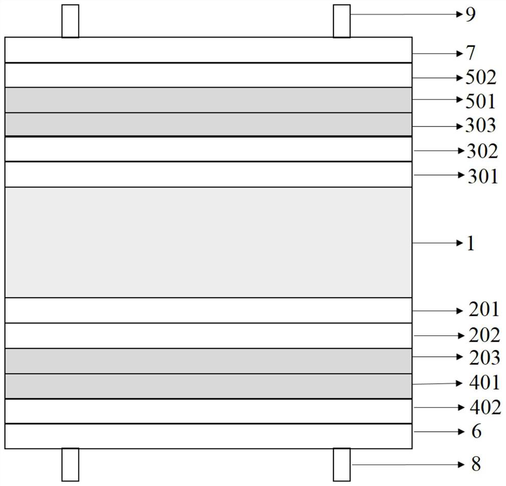
[0043] combine figure 1 , a high-efficiency silicon heterojunction solar cell of the present embodiment comprises an N-type crystalline silicon wafer 1, and the front side of the N-type crystalline silicon wafer 1 is sequentially provided with thin layers of SiO 2 Layer 301, hydrogenated amorphous silicon oxycarbide film layer 302, C-doped SiO 2 Layer 303, amorphous silicon doped N-type layer, TCO conductive layer 7 and electrode 9; the back of the N-type crystalline silicon wafer 1 is sequentially provided with a thin layer of SiO 2 Layer 201, hydrogenated amorphous silicon oxycarbide film layer 202, C-doped SiO 2 layer 203 , amorphous silicon doped P-type layer, TCO conductive layer 6 and electrode 8 . in,

[0044] The high-quality thin-layer SiO 2 The layer has a thickness of 1 nm and passivates the surface of the silicon substrate.

[0045] The thickness of the hydrogenated amorphous silicon oxycarbide thin film layer is 2nm. In the present embodiment, the hydrogenate...

Embodiment 2

[0052] A high-efficiency silicon heterojunction solar cell in this embodiment is basically the same as in Embodiment 1, except that the high-quality thin-layer SiO 2 The thickness of the layer is 3 nm. The thickness of the hydrogenated amorphous silicon oxycarbide film layer is 10nm, the non-stoichiometric ratio x of the hydrogenated amorphous silicon oxycarbide film is 0.95, the non-stoichiometric ratio y is 0.05, and the band gap is 1.7eV. The C-doped SiO 2 The thickness of the layer is 5 nm. The thickness of the amorphous silicon-doped P-type layer is 30nm, the thickness of the amorphous silicon-doped N-type layer is 30nm; the thickness of the TCO conductive layer is 110nm.

Embodiment 3

[0054] combine figure 1 , a high-efficiency silicon heterojunction solar cell of the present embodiment comprises an N-type crystalline silicon wafer 1, and the front side of the N-type crystalline silicon wafer 1 is sequentially provided with thin layers of SiO 2 Layer 301, hydrogenated amorphous silicon oxycarbide film layer 302, C-doped SiO 2 Layer 303, amorphous silicon doped N-type layer, TCO conductive layer 7 and electrode 9; the back of the N-type crystalline silicon wafer 1 is sequentially provided with a thin layer of SiO 2 Layer 201, hydrogenated amorphous silicon oxycarbide film layer 202, C-doped SiO 2 layer 203 , amorphous silicon doped P-type layer, TCO conductive layer 6 and electrode 8 . in,

[0055] The high-quality thin-layer SiO 2 The layer has a thickness of 2 nm and passivates the surface of the silicon substrate.

[0056] The thickness of the hydrogenated amorphous silicon oxycarbide film layer is 5nm, the non-stoichiometric ratio x of the hydrogena...


PUM

PropertyMeasurementUnit
Thicknessaaaaaaaaaa
Thicknessaaaaaaaaaa
Bandgap widthaaaaaaaaaa

Abstract

The invention discloses an efficient silicon heterojunction solar cell and a preparation method thereof, and belongs to the technical field of solar cells. A thin SiO2 layer, a hydrogenated amorphous silicon oxycarbide thin film layer, a C-doped SiO2 layer, an amorphous silicon doped N-type layer, a TCO conductive layer and an electrode are sequentially arranged on the front surface of an N-type crystal silicon wafer of the battery; a thin SiO2 layer, a hydrogenated amorphous silicon oxycarbide thin film layer, a C-doped SiO2 layer, an amorphous silicon doped P-type layer, a TCO conductive layer and an electrode are sequentially arranged on the back surface of the substrate; and the amorphous silicon doped P-type layer comprises a light B-doped amorphous silicon layer and a heavy B-doped amorphous silicon layer. According to the heterojunction solar cell with the hydrogenated amorphous carbon silicon oxide thin film as the intrinsic passivation layer, the excellent passivation effect on the crystalline silicon surface is achieved, and interface carrier recombination is reduced; and meanwhile, an improved double-diffusion B process is adopted, so that reduction of forbidden bandwidth and unnecessary passive film doping caused by diffusion of B atoms to the intrinsic amorphous silicon layer during B2H6 doping are prevented, and the conversion efficiency of the silicon heterojunction battery is improved.

Description

technical field [0001] The invention relates to the technical field of solar cells, in particular to a high-efficiency silicon heterojunction solar cell and a preparation method thereof. Background technique [0002] At present, the mainstream battery product in the market is the P-type monocrystalline PERC battery, and the efficiency of the P-type PERC battery has reached the upper limit. However, with the demand of the market and the continuous development of industry technology, N-type crystalline silicon solar cell technology has received more and more attention in recent years, mainly including passivated emitter back surface fully diffused cells (n-PERT), tunnel oxide Passivated contact cells (TOPCon) and heterojunction cells (HJT), N-type crystalline silicon solar cells have further improved the conversion efficiency of crystalline silicon solar cells. [0003] The structure of the existing HJT battery is to make a layer of amorphous silicon intrinsic layer and doped...

Claims


Application Information

Patent Timeline
IPC IPC(8): H01L31/0216H01L31/0224H01L31/0747H01L31/18H01L31/20
CPCH01L31/02167H01L31/022425H01L31/0747H01L31/1804H01L31/1868H01L31/202H01L31/022466H01L31/1884
Inventor 王锦乐肖俊峰
Owner TONGWEI SOLAR ENERGY CHENGDU CO LID
Why Eureka
Try Eureka