Pre-diffusion film for passivating contact structure and its preparation method and application
A pre-diffusion sheet, contact structure technology, applied in the direction of final product manufacturing, sustainable manufacturing/processing, climate sustainability, etc. Increase the surface recombination rate and other issues to improve the surface passivation effect, reduce the content of metal impurities in the body, and reduce the effect of transition dependence
- Summary
- Abstract
- Description
- Claims
- Application Information
AI Technical Summary
Problems solved by technology
Method used
Image
Examples
Embodiment 1
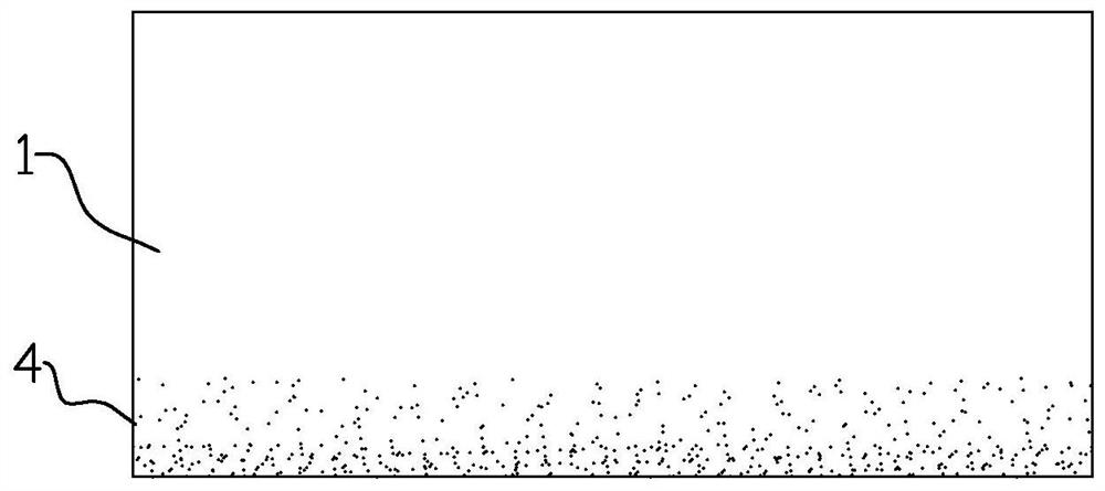
[0038] This embodiment provides a pre-diffuser, such as image 3 Shown, in order to form pre-diffusion impurity layer 4 by pre-diffusion doping impurity on the surface of silicon chip 1, pre-diffusion doping impurity can be phosphorus, boron etc., the preparation of pre-diffusion sheet is illustrated below with phosphorus as example, boron doping The preparation principle and method of the pre-diffusion sheet are similar to those of phosphorus doping.
[0039] Method 1: Clean the silicon wafer 1, put it into a tube annealing furnace, and use POCl 3 Perform high-temperature diffusion treatment for the phosphorus source, then remove the phosphosilicate glass layer and the phosphorus-rich layer, and finally clean the surface to obtain a pre-diffusion sheet.
[0040] Method 2: Clean the silicon wafer 1, apply a layer of phosphorus source on the surface of the silicon wafer 1 by spraying, spin coating, printing, printing and other methods, then anneal at high temperature to diffus...
Embodiment 2
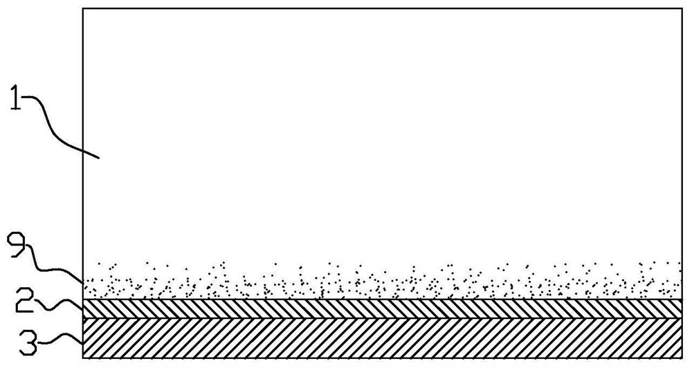
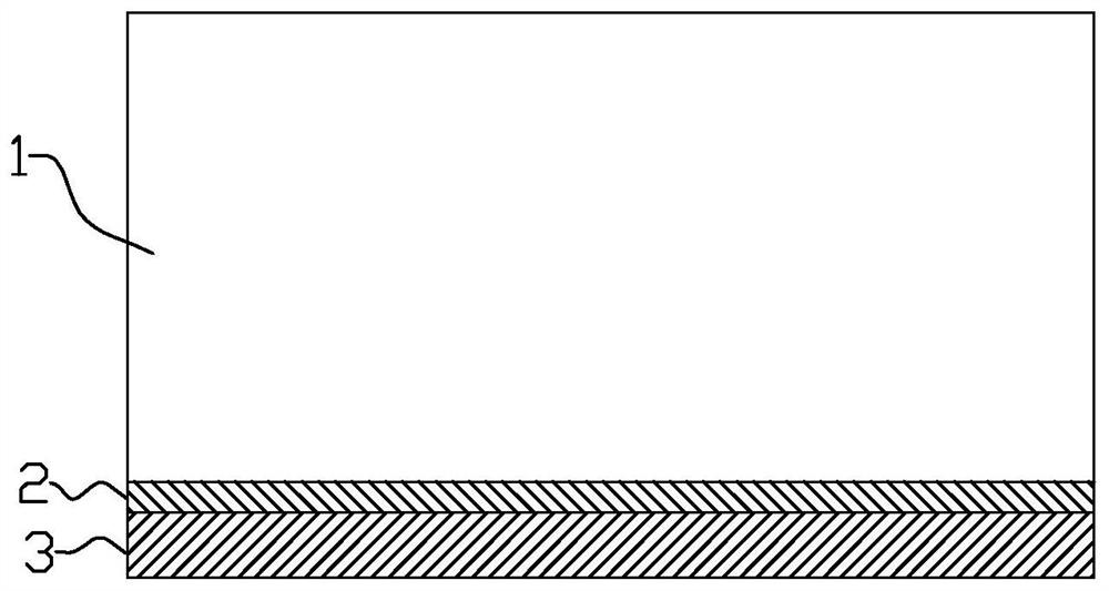
[0042] This embodiment provides a method for making a passivation contact structure using the above-mentioned pre-diffusion sheet, and the structure diagram of the passivation contact structure prepared is as follows Figure 4 shown.
[0043] The preparation method of the pre-diffusion TOPCon passivation structure: clean the surface of the pre-diffusion sheet, and then sequentially deposit a layer of ultra-thin silicon oxide (the first covering layer 2) with a thickness usually less than 2 nanometers, a layer of n-type or p-type doped Miscellaneous polysilicon thin film (second covering layer 3), wherein silicon oxide is prepared by hot nitric acid method; finally high-temperature annealing is carried out at 800-900°C, specifically, the high-temperature annealing temperature of n-type silicon wafer is 800-850°C, p The high-temperature annealing temperature of the type silicon wafer is 850-900°C, and then the metal electrodes are deposited.
[0044]The preparation method of th...
Embodiment 3
[0049] This embodiment provides a method for preparing a crystalline silicon battery using the above-mentioned pre-diffusion sheet.
[0050] Preparation method of pre-diffusion TOPCon crystalline silicon battery (Take n-type pre-diffusion TOPCon crystalline silicon battery as an example, the preparation principle and method of p-type crystalline silicon battery can refer to n-type): n-type silicon wafer 1 surface cleaning, texturing, surface Boron expansion, chemical polishing on the back side, pre-diffusion on the back side, etch cleaning, preparation of silicon oxide (first cover layer 2) and doped polysilicon (second cover layer 3) on the back side, high temperature crystallization, preparation of passivation and anti-reflection stacks on the front side 6 and the emitter 7, the back can be coated with a silicon nitride layer, double-sided metallized to form a metal electrode 5, wherein at least the front metal electrode 5 forms a metal grid line. After the battery was fabri...
PUM
| Property | Measurement | Unit |
|---|---|---|
| electrical resistivity | aaaaa | aaaaa |
| electrical resistivity | aaaaa | aaaaa |
| thickness | aaaaa | aaaaa |
Abstract
Description
Claims
Application Information


