
Vertical back incidence coplanar electrode high-power photoconductive switch

A photoconductive switch and back-incidence technology, applied in the direction of circuits, capacitors, electrical components, etc., can solve the problems of high laser excitation power, easy damage, and small current cross section

Active Publication Date: 2021-05-18
SHANGHAI SPACEFLIGHT ELECTRONICS & COMM EQUIP RES INST
View PDF9 Cites 0 Cited by
  • Summary
  • Abstract
  • Description
  • Claims
  • Application Information

AI Technical Summary

Problems solved by technology

In the nonlinear (avalanche) working mode, one photon excites multiple electron-hole pairs to produce an avalanche effect. When the laser disappears, the avalanche effect continues for a period of time and ends, which is called the "Lock on" effect, and the recovery time is slow. Advantages The laser excitation power is small; in the linear working mode, the photons correspond to the excited electron-hole pairs one by one. When the laser excitation disappears, the electron-hole pairs match instantaneously. The disadvantage is that the laser excitation power is large.
[0004] The advantage of the photoconductive switch of the same surface electrode is that the "Triple point" effect is small; the disadvantage is that the current cross section is small and uneven, the current density is high, and it is easy to damage; the same surface electrode is also easy to break down; the optical path is short, resulting in low photon quantum efficiency

Method used


Image

  • Vertical back incidence coplanar electrode high-power photoconductive switch
  • Vertical back incidence coplanar electrode high-power photoconductive switch
  • Vertical back incidence coplanar electrode high-power photoconductive switch

Examples


Embodiment Construction

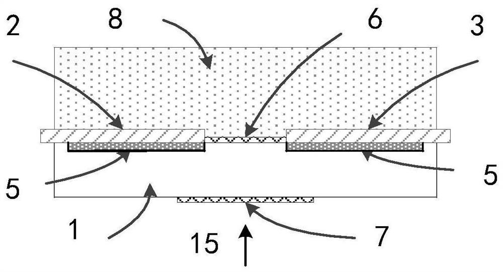
[0054] In order to more clearly illustrate the embodiments of the present invention or the technical solutions in the prior art, the specific implementation manners of the present invention will be described below with reference to the accompanying drawings. Obviously, the accompanying drawings in the following description are only some embodiments of the present invention, and those skilled in the art can obtain other accompanying drawings based on these drawings and obtain other implementations.

[0055] In order to make the drawing concise, each drawing only schematically shows the parts related to the present invention, and they do not represent the actual structure of the product. In addition, to make the drawings concise and easy to understand, in some drawings, only one of the components having the same structure or function is schematically shown, or only one of them is marked. Herein, "a" not only means "only one", but also means "more than one".

[0056] A high-pow...


PUM


Abstract

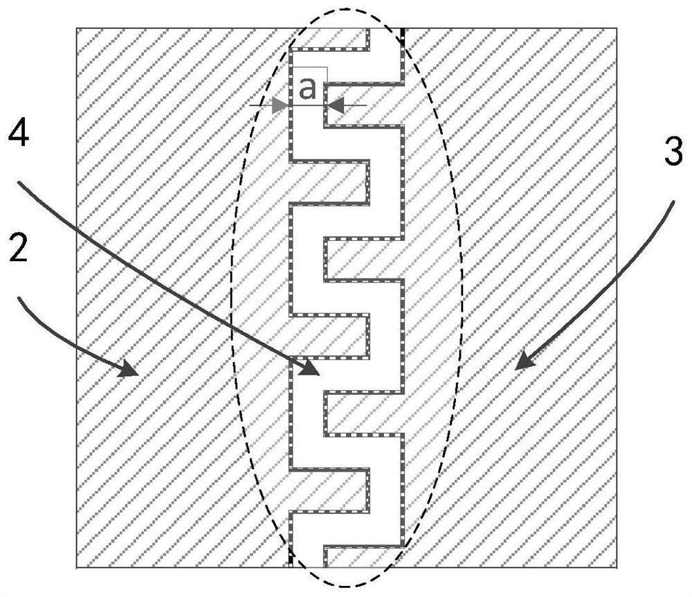
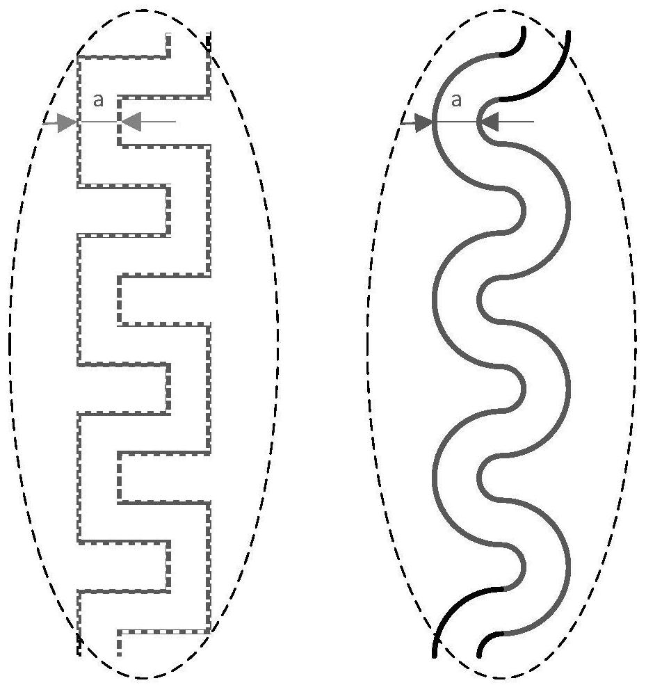
The invention discloses a vertical back incidence coplanar electrode high-power photoconductive switch. The photoconductive switch comprises a semiconductor wafer, an input electrode and an output electrode, wherein the input electrode and the output electrode are arranged on the front surface of the semiconductor wafer; and the input electrodes and the output electrodes are arranged at intervals, adjacent edges are staggered to form an interdigital structure, and the interdigital structure is a shaped irradiation photosensitive area of the photoconductive switch. The adjacent edges of the input electrode and the output electrode are mutually staggered to form an interdigital structure, so that the contact length between the electrodes is prolonged, the on resistance of the photoconductive switch is effectively reduced, the input electrode and the output electrode can be arranged side by side or annularly, and the annular arrangement mode prolongs the contact length between the electrodes on the basis of the interdigital structure, further reduces the on-resistance of the photoconductive switch, and greatly improves the performance of the photoconductive switch.

Description

technical field [0001] The invention belongs to the technical field of photoconductive switches, in particular to a high-power photoconductive switch with vertical back-incidence electrodes on the same plane. Background technique [0002] Photoconductive switches are called photoconductive semiconductor switches (PCSS), which use laser pulses to trigger photoconductive semiconductor solid-state switches. They have high power (MW level), fast response speed (~10ps-~100ps level), low trigger jitter ( PS level), strong anti-electromagnetic interference ability, small size, easy integration and other advantages, it has broad application prospects in high-current ignition devices, high-power transient testing, impact radar and electromagnetic interference. [0003] The photoconductive switch has two working modes. In the nonlinear (avalanche) working mode, one photon excites multiple electron-hole pairs to produce an avalanche effect. When the laser disappears, the avalanche eff...

Claims


Application Information

Patent Timeline
Patent Type & Authority Applications(China)
IPC IPC(8): H01L31/0224H01L31/0216H01L31/0232H01L31/024H01L31/02H01L31/08H01L23/64
CPCH01L31/0224H01L31/02002H01L31/02327H01L31/0216H01L31/024H01L31/08H01L28/40H01L31/02016
Inventor 姚崇斌袁涛尚吉扬罗燕王立春李培丁海洋
Owner SHANGHAI SPACEFLIGHT ELECTRONICS & COMM EQUIP RES INST
Learn More