

ALD machining equipment and method
A technology of processing equipment and heaters, applied in metal material coating process, gaseous chemical plating, coating and other directions, can solve the problems of poor uniformity of deposited film, waste of precursor source, difficult quality assurance, etc. The effect of improving utilization and reducing volume
- Summary
- Abstract
- Description
- Claims
- Application Information
AI Technical Summary
Problems solved by technology
Method used
Image

Examples
Embodiment 1
[0052] This embodiment discloses an ALD processing equipment.
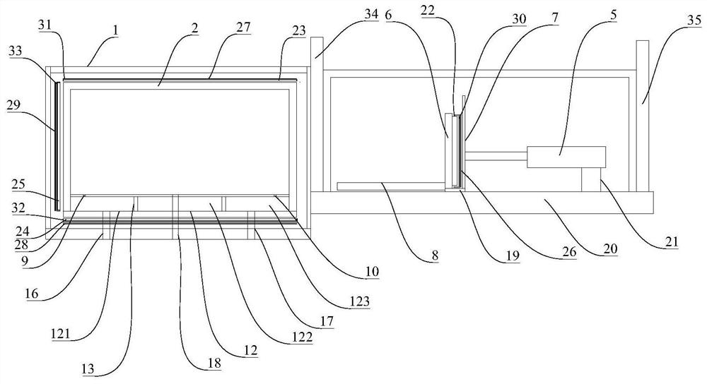
[0053] figure 1 It is a structural schematic diagram of a kind of ALD processing equipment of the present embodiment, combined with figure 1 , the ALD processing equipment of this embodiment includes a reactor, a feeding chamber and a conveying device.
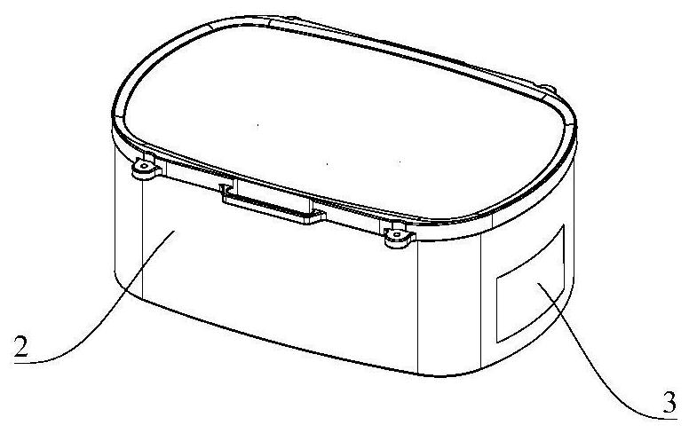
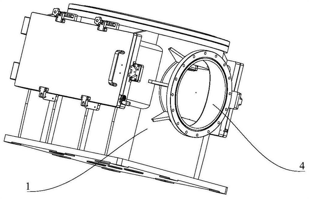
[0054] combine figure 1 , the reactor of this embodiment includes a vacuum chamber 1 and a reaction chamber 2, and the reaction chamber 2 is built in the vacuum chamber 1.
[0055] figure 2 It is a structural schematic diagram of the vacuum chamber of this embodiment, image 3 It is a structural schematic diagram of the reaction chamber of the present embodiment, combined with Figure 1-Figure 3 , the side wall of the reaction chamber 2 of the present embodiment is provided with a first feed port 3, the side wall of the vacuum chamber 1 is provided with a second feed port 4, and the first feed port 3 and the second feed port 4 are located in the reaction cha...
Embodiment 2
[0061] This embodiment provides a reaction chamber suitable for the ALD processing equipment shown in Embodiment 1.
[0062] Figure 4 It is a schematic top view of the reaction chamber of this embodiment, combined with image 3 as well as Figure 4 The bottom of the reaction chamber 2 in this embodiment is provided with an inlet channel 9 and an outlet channel 10 , and the inlet channel 9 and the outlet channel 10 are arranged opposite to each other at the center line of the bottom of the reaction chamber 2 .
[0063] During specific implementation, the precursor source is injected into the reaction chamber 2 from the inlet channel 9 of the reaction chamber 2, and is discharged from the gas outlet channel 10 of the reaction chamber 2, because the gas inlet channel 9 and the gas outlet channel 10 react with each other. The center line of the bottom of the chamber 2 is relatively arranged, therefore, the fluid field in the reaction chamber 2 is a laminar flow, and the intake ...
Embodiment 3
[0068] This embodiment provides a reaction chamber suitable for the ALD processing equipment shown in Embodiment 1 or 2.
[0069] Figure 5 It is a structural schematic diagram of the reaction chamber of Example 3. The difference between the reaction chamber shown in this embodiment and the reaction chamber shown in Example 2 is that two gas uniform plates 11 are arranged in the reaction chamber 2, Two gas uniform plates 11 are oppositely arranged with the center line of the bottom of the reaction chamber 2, and the two gas uniform plates 11 are arranged between the inlet channel 9 and the gas outlet channel 10, and the two gas uniform plates 11 divide the reaction chamber into For the air inlet chamber, the reaction chamber and the air outlet chamber, each gas uniform plate 11 is provided with a plurality of through holes.
[0070] The precursor source can enter the inlet chamber through the inlet channel 9, and then enter the reaction chamber through the uniform gas plate 1...
PUM
| Property | Measurement | Unit |
|---|---|---|
| Thickness | aaaaa | aaaaa |
Abstract
Description
Claims
Application Information