Conductive particle filled polymer layered composite dielectric material and preparation method thereof
A filling polymer, layered composite technology, applied in the field of dielectric materials, can solve the problems of unfavorable high dielectric, uniform dispersion of chemical coating on the surface, sensitive filler content range, etc., to achieve high dielectric constant, promote Interfacial polarization, the effect of reducing conductivity loss
- Summary
- Abstract
- Description
- Claims
- Application Information
AI Technical Summary
Problems solved by technology
Method used
Image
Examples
Embodiment 1
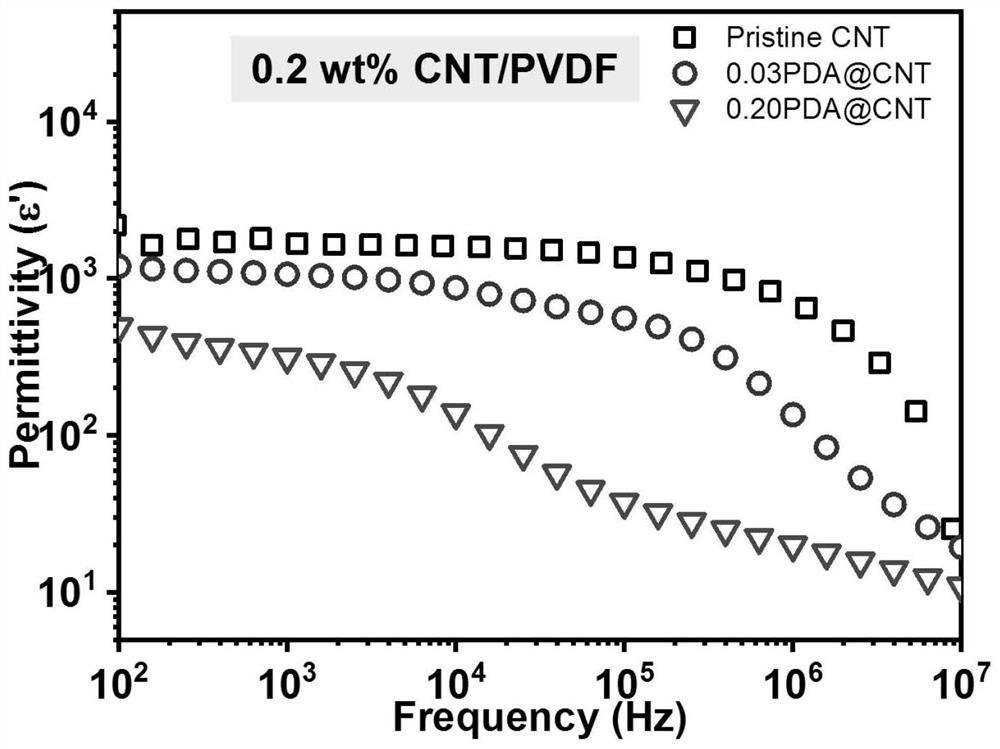
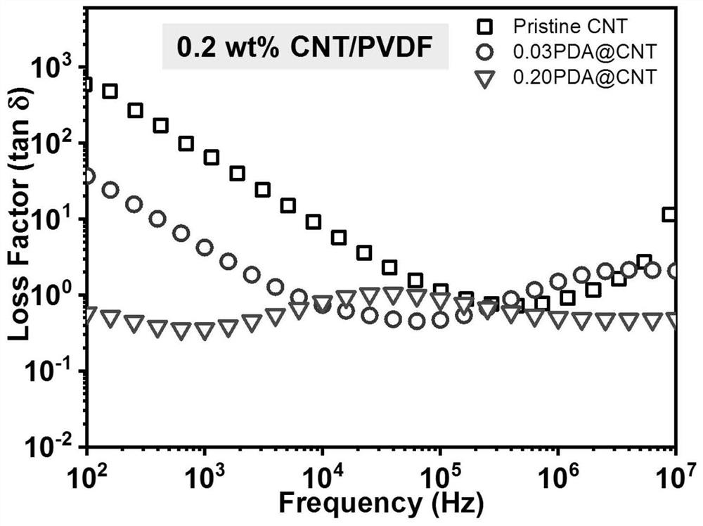
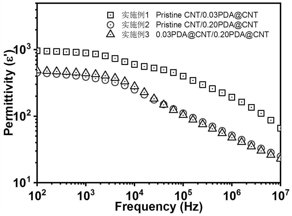
[0038] A polymer multilayer composite dielectric material filled with conductive particles, consisting of polyvinylidene fluoride (PVDF) resin, multi-walled carbon nanotubes (Pristine CNT) and polydopamine-coated modified carbon nanotubes (PDA@CNT) , its multi-layer structure is an A / B / A / B multi-layer structure in which conductive layers (A) / dielectric layers (B) are alternately compounded. The total number of layers is 4 layers, the total thickness is 0.8mm, and the thickness of a single layer is 0.2mm.
[0039] Wherein the conductive layer is a blend of polyvinylidene fluoride (PVDF) / multi-walled carbon nanotubes (Pristine CNT), and its raw material composition mass ratio is:
[0040] Polyvinylidene fluoride (PVDF) 99.8%
[0041] Multi-walled carbon nanotubes (Pristine CNT) 0.2%
[0042] The dielectric layer is a blend of polyvinylidene fluoride (PVDF) / polydopamine surface-coated modified carbon nanotubes (PDA@CNT), and its raw material composition mass ratio is:
[0043]...
Embodiment 2
[0050] A polymer multilayer composite dielectric material filled with conductive particles, consisting of polyvinylidene fluoride (PVDF) resin, multi-walled carbon nanotubes (Pristine CNT) and polydopamine-coated modified carbon nanotubes (PDA@CNT) , is characterized in that, its multi-layer structure is the A / B / A / B multi-layer structure of conducting layer (A) / dielectric layer (B) alternate compounding, and its total number of layers is 4 layers, and total thickness is 0.8mm, The single layer thickness is 0.2mm.
[0051] Wherein the conductive layer is a blend of polyvinylidene fluoride (PVDF) / multi-walled carbon nanotubes (Pristine CNT), and its raw material composition mass ratio is:
[0052] Polyvinylidene fluoride (PVDF) 99.8%
[0053] Multi-walled carbon nanotubes (Pristine CNT) 0.2%
[0054] The dielectric layer is a blend of polyvinylidene fluoride (PVDF) / polydopamine surface-coated modified carbon nanotubes (PDA@CNT), and its raw material composition mass ratio is: ...
Embodiment 3
[0062] A conductive particle-filled polymer multilayer composite dielectric material, which is composed of polyvinylidene fluoride (PVDF) resin and polydopamine surface-coated modified carbon nanotubes (PDA@CNT), and its multilayer structure is a conductive layer (A ) / dielectric layer (B) alternate composite A / B / A / B multilayer structure, the total number of layers is 4 layers, the total thickness is 0.8mm, and the single layer thickness is 0.2mm.
[0063] The conductive layer and the dielectric layer in the multilayer composite dielectric material are blends of polyvinylidene fluoride (PVDF) / polydopamine surface-coated modified carbon nanotubes (PDA@CNT), and the mass ratio of the raw materials is:
[0064] Polyvinylidene fluoride (PVDF) 99.8%
[0065] Polydopamine-coated modified carbon nanotubes (PDA@CNT) 0.2%
[0066] Polydopamine surface-coated modified carbon nanotubes (PDA@CNT) are prepared by the preparation method of polydopamine surface-coated carbon nanotubes, where...
PUM
| Property | Measurement | Unit |
|---|---|---|
| thickness | aaaaa | aaaaa |
| pore size | aaaaa | aaaaa |
| length | aaaaa | aaaaa |
Abstract
Description
Claims
Application Information


