Array type pressure measuring device
A measuring device and array technology, applied in the direction of fluid pressure measurement by changing ohmic resistance, can solve the problem of inaccurate characterization of the temperature state of piezoresistive sensitive chips, complex thermodynamic characteristics of ceramic chip-PCB stack, and limited temperature compensation accuracy To achieve the effect of maintaining long-term stability and comprehensive accuracy, helping heat dissipation management, and reducing assembly stress
- Summary
- Abstract
- Description
- Claims
- Application Information
AI Technical Summary
Problems solved by technology
Method used
Image
Examples
Embodiment 2
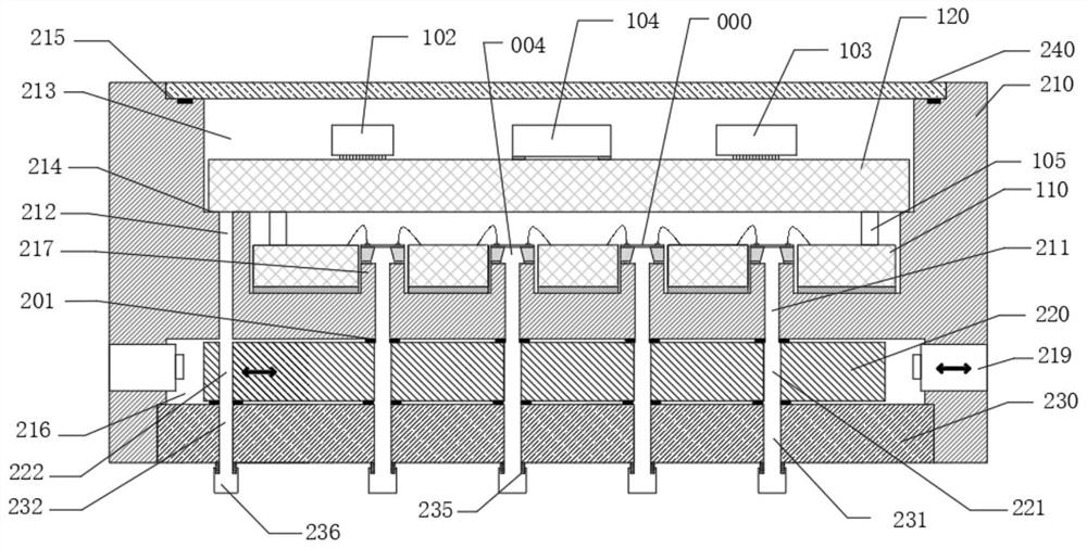
[0062] refer to Figure 14 , 15 The difference between this embodiment and Embodiment 1 is that the second alloy substrate 220 and the third alloy substrate 230 are placed in the open cavity 217 on the same side of the first alloy substrate 210, or they can be divided into two parts and placed in the first alloy substrate respectively. The two sides of the alloy substrate 210; the air guide hole 211 is converted according to the position of the second alloy substrate 220, and the direct air guide hole structure in embodiment 1 is connected to the front and back of the first alloy substrate 210. The guide air hole in this embodiment The gas holes 211 communicate with the front surface of the first alloy substrate 210 and the same or different sides; for the rest, refer to Example 1.
Embodiment 3
[0064] refer to Figure 16 The difference between this embodiment and Embodiment 1 is that the first circuit chip 110 is placed in the front open cavity 212 of the first alloy substrate 210 during assembly, and the second circuit chip 120 is placed in the front open cavity 212 of the first alloy substrate 210. The open cavity 215 on the back is connected by bonding or bolts respectively, which is convenient for maintenance and replacement. The second alloy substrate 220 and the third alloy substrate 230 are placed in the open cavity 217 on the same side of the first alloy substrate 210, or they can be divided into two parts and placed on both sides of the first alloy substrate 210 respectively, The air guide holes 130 are converted according to the position of the second alloy substrate, as in Embodiment 2; the top and bottom of the first alloy substrate 210 are respectively provided with a fourth alloy substrate 240 for sealing open cavities; the rest refer to Embodiment 1. ...
Embodiment 4
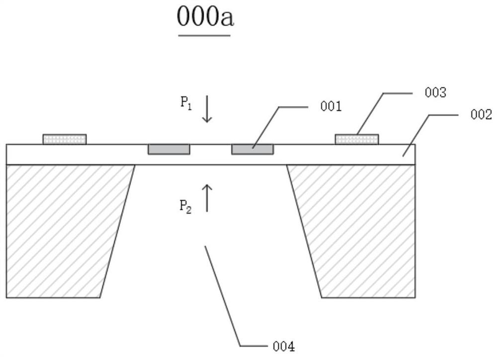
[0066] refer to Figure 17, the piezoresistive sensitive chip in this embodiment is an absolute pressure piezoresistive sensitive chip 000c. Resistor 001, passivation layer 002, Pad 003 and solder ball 006; an open cavity 004 is formed on the back of the piezoresistive sensitive chip 000c by etching; after vacuuming the open cavity 004 on the back, another piece of silicon or glass 010 is bonded to the back of the piezoresistive sensitive chip 000c to seal the open cavity 004 to form an absolute pressure piezoresistive sensitive chip 000c. Among them, Pad 004 includes at least 1 power pad, 1 ground pad, and 2 signal pads.
[0067] In order to be compatible with the assembly system described in Embodiment 1, solder balls are formed on the front side of the piezoresistive sensitive chip 000 and flip-chip soldered on the interconnect substrate 020 with air guide holes, on which there are electrical wiring layers and corresponding solder balls. Welding pad; then use SU8 or BCB g...
PUM
 Abstract
Description
Claims
Application Information


