Three-dimensional integrated interlayer optical interconnection structure and forming method thereof
An integrated layer, optical interconnection technology, applied in the directions of light guides, optics, optical components, etc., can solve the problems of difficult and low-loss transmission of optical signals, and achieve the effect of wide application range, high integration, and high extinction ratio
- Summary
- Abstract
- Description
- Claims
- Application Information
AI Technical Summary
Problems solved by technology
Method used
Image

Examples
Embodiment 1
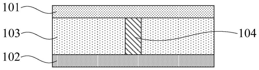
[0050] See figure 1 with figure 2 This embodiment provides a three-dimensional integrated interlayer optical interconnection structure including: the first functional material layer 101, the optical isolation layer 103, the second functional material layer 102 and the inter-layer waveguide 104 ;
[0051] The first functional material layer 101 is isolated between the light isolation layer 103 between the second functional material layer 102;
[0052] The inter-layer waveguide 104 is located in the light isolation layer 103 and connects the first functional material layer 101 and the second functional material layer 102;
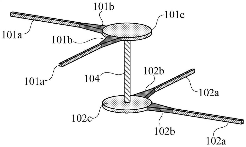
[0053]The first functional material layer 101 includes a first optical waveguide trip 101a, a first wedge-shaped waveguide 101b, and a first grating coupling waveguide 101c, the first wedge waveguide 101b connected to the first optical waveguide 101a and the first The raster coupling waveguide 101c, the first grating coupling waveguide 101c connects the inter-lay...
Embodiment 2
[0074] This embodiment provides a method of forming a three-dimensional integrated interlayer optical interconnection structure, comprising the steps of:
[0075] Provide a substrate;
[0076] A graphized first functional material layer 101 is formed on the substrate, and the first functional material layer 101 includes a first optical waveguide 101a, a first wedge waveguide 101b, and a first grating coupling waveguide 101c, said first The wedge waveguide 101b connects the first optical waveguide 101a and the first grating coupling waveguide 101c;
[0077] The optical isolation layer 103 is formed on the first functional material layer 101, and an inter-layer waveguide 104 is formed in the optical spacer layer 103, and the first grating coupling waveguide 101c connects the intermodulation waveguide 104;
[0078] A graphical second functional material layer 102 is formed on the light isolation layer 103, and the second functional material layer 102 includes a second optical wavegui...
PUM
| Property | Measurement | Unit |
|---|---|---|
| thickness | aaaaa | aaaaa |
| width | aaaaa | aaaaa |
| depth | aaaaa | aaaaa |
Abstract
Description
Claims
Application Information
 - R&D
- Intellectual Property
- Life Sciences
- Materials
- Tech Scout
- Unparalleled Data Quality
- Higher Quality Content
- 60% Fewer Hallucinations
Browse by: Latest US Patents, China's latest patents, Technical Efficacy Thesaurus, Application Domain, Technology Topic, Popular Technical Reports.
© 2025 PatSnap. All rights reserved.Legal|Privacy policy|Modern Slavery Act Transparency Statement|Sitemap|About US| Contact US: help@patsnap.com