
Manufacturing method of semiconductor structure and semiconductor structure

A manufacturing method and semiconductor technology, applied in semiconductor/solid-state device manufacturing, semiconductor devices, transistors, etc., can solve problems such as short circuit of upper and lower electrodes of capacitors, affecting the electrical performance of semiconductor structures, and difficulty in controlling the dimensional accuracy of capacitor holes.

Active Publication Date: 2021-06-08
CHANGXIN MEMORY TECH INC
View PDF12 Cites 2 Cited by
  • Summary
  • Abstract
  • Description
  • Claims
  • Application Information

AI Technical Summary

Problems solved by technology

[0003] With the shrinking of memory technology nodes, the aspect ratio of the capacitor hole used to make the lower electrode of the capacitor gradually increases. When the capacitor hole is formed by etching, the capacitor The dimensional accuracy of the hole is difficult to control, and it is easy to form a slit at the bottom of the capacitor hole, which is not conducive to the subsequent formation of the upper and lower electrodes of the capacitor completely separated by the dielectric layer on the basis of the capacitor hole, which will easily lead to a short circuit between the upper and lower electrodes of the capacitor, thus affecting the semiconductor. Electrical properties of the structure

Method used


Image

  • Manufacturing method of semiconductor structure and semiconductor structure
  • Manufacturing method of semiconductor structure and semiconductor structure
  • Manufacturing method of semiconductor structure and semiconductor structure

Examples


Embodiment Construction

[0026] It can be seen from the background art that the yield rate and electrical performance of the semiconductor structure in the prior art need to be improved.

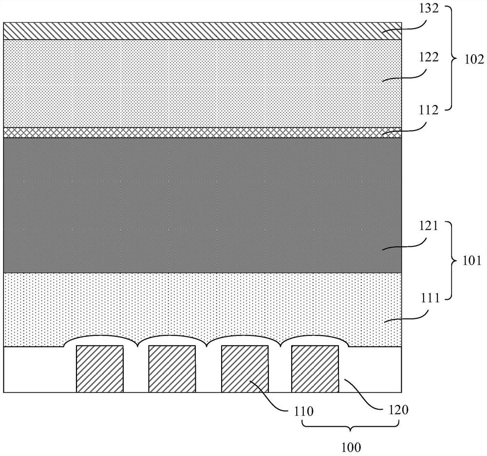
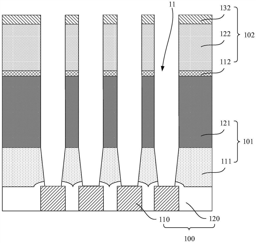
[0027] It is found through analysis that in order to form capacitor holes with a large aspect ratio, a first mask layer and a second mask layer are usually sequentially formed on the first support layer, and the first mask layer is generally a single-layer structure. Etching part of the second mask layer, part of the first mask layer and part of the first support layer until the capacitive contact structure is exposed to form the capacitive hole, due to the gap between the mask plate used to form the capacitive hole and the capacitive contact structure The alignment error and the over-etching of the first supporting layer by the etching process easily make the opening size of the bottom of the capacitor hole larger than the opening size of the top of the capacitor hole. Specifically, the intersection of the side wal...


PUM

PropertyMeasurementUnit
Angleaaaaaaaaaa

Abstract

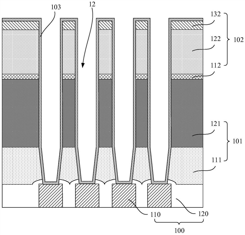
The embodiment of the invention provides a manufacturing method of a semiconductor structure and the semiconductor structure, and the manufacturing method comprises the steps: providing a substrate which is provided with a plurality of capacitor contact structures which are arranged at intervals and a first supporting layer which covers the capacitor contact structures; forming a first mask layer and a second mask layer sequentially on the first supporting layer, wherein the first mask layer at least comprises a first dielectric layer and a second dielectric layer which are sequentially formed; removing a part of the first mask layer, a part of the second mask layer and a part of the first supporting layer by using an etching process to form a first capacitor hole exposing a part of the capacitor contact structure, wherein under the same etching condition, the transverse etching rate of the first dielectric layer is smaller than that of the second dielectric layer; and forming a lower electrode layer on the bottom and the side wall of the first capacitor hole. According to the embodiment of the invention, the yield of the semiconductor structure and the electrical performance of the semiconductor structure are improved.

Description

technical field [0001] Embodiments of the present invention relate to the field of semiconductors, and in particular, to a method for fabricating a semiconductor structure and the semiconductor structure. Background technique [0002] Memory is a memory component used to store programs and various data information. According to the type of memory used, it can be divided into read-only memory and random access memory. A memory usually includes a capacitor and a transistor connected to the capacitor. The capacitor is used to store charges representing stored information. The transistor is a switch that controls the charge flow into and out of the capacitor. [0003] With the continuous shrinking of the memory process node, since the aspect ratio of the capacitor hole used to make the lower electrode of the capacitor gradually increases, when the capacitor hole is formed by etching, the dimensional accuracy of the capacitor hole is difficult to control, and it is easy to form a...

Claims


Application Information

Patent Timeline
IPC IPC(8): H01L21/8242H01L27/108
CPCH10B12/30H10B12/03H10B12/033H01L28/90H01L27/01
Inventor 张海龙
Owner CHANGXIN MEMORY TECH INC
Learn More