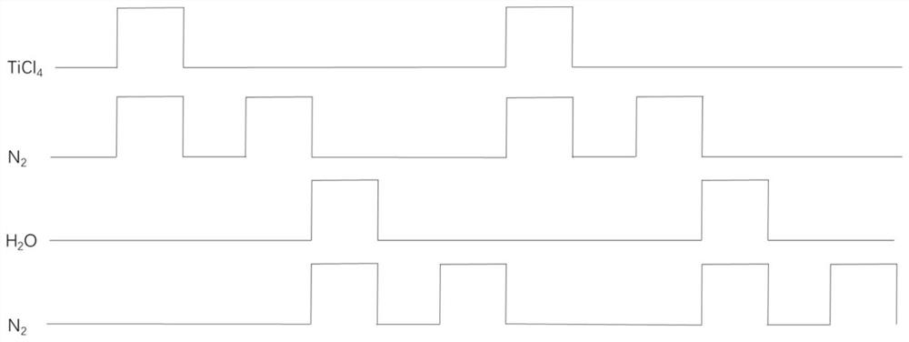
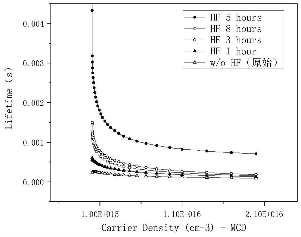
Preparation method of silicon surface passivation layer
A passivation layer and silicon surface technology, which is applied in coating, gaseous chemical plating, final product manufacturing, etc., can solve the problems of high cost of energy-consuming equipment and high equipment cost
- Summary
- Abstract
- Description
- Claims
- Application Information
AI Technical Summary
Problems solved by technology
Method used
Image
Examples
Embodiment 1
[0034] Embodiment 1, the preparation of silicon surface passivation layer
[0035] 1. Cleaning
[0036] (1) Immerse the raw silicon wafer (melted silicon wafer in the double-sided polishing area, resistivity 1-5 ohm cm, thickness 280 μm, φ2 inch) into H with a volume ratio of 3:1 2 SO 4 and H 2 o 2 In the mixed solution, heat to 100 degrees Celsius and keep warm for 15 minutes; take out the silicon wafer and rinse it with deionized water for 2 minutes;
[0037] (2) Immerse the silicon wafer cleaned in step (1) in NH with a volume ratio of 1:1:5 4 OH, H 2 o 2 , in a mixed solution of deionized water, heated to 80 degrees Celsius, and kept for 15 minutes; take out the silicon wafer, and rinse it with deionized water for 2 minutes;
[0038] (3) immerse the silicon wafer after step (2) cleaning into HCl, H with a volume ratio of 1:1:5 2 o 2 , in a mixed solution of deionized water, heated to 80 degrees Celsius, and kept for 15 minutes; take out the silicon wafer, and rins...
PUM
| Property | Measurement | Unit |
|---|---|---|
| Thickness | aaaaa | aaaaa |
Abstract
Description
Claims
Application Information
 - R&D Engineer
- R&D Manager
- IP Professional
- Industry Leading Data Capabilities
- Powerful AI technology
- Patent DNA Extraction
Browse by: Latest US Patents, China's latest patents, Technical Efficacy Thesaurus, Application Domain, Technology Topic, Popular Technical Reports.
© 2024 PatSnap. All rights reserved.Legal|Privacy policy|Modern Slavery Act Transparency Statement|Sitemap|About US| Contact US: help@patsnap.com


