Silica nanoarray with controllable morphology, preparation method and application thereof

A silicon dioxide and nanoarray technology, applied in the field of nanomaterials, can solve the problems of complex processing process and difficult to control surface structure, etc.

Active Publication Date: 2022-07-22
FUDAN UNIV
View PDF0 Cites 0 Cited by
  • Summary
  • Abstract
  • Description
  • Claims
  • Application Information

AI Technical Summary

Problems solved by technology

[0002] The nano-biological interaction is affected by the surface structure of the substrate, but some existing methods (such as chemical etching process, electrochemical deposition, chemical vapor deposition), the processing process is often complicated, and it is difficult to precisely control the surface structure at the nanoscale

Method used


Image

  • Silica nanoarray with controllable morphology, preparation method and application thereof
  • Silica nanoarray with controllable morphology, preparation method and application thereof
  • Silica nanoarray with controllable morphology, preparation method and application thereof

Examples


Embodiment 1

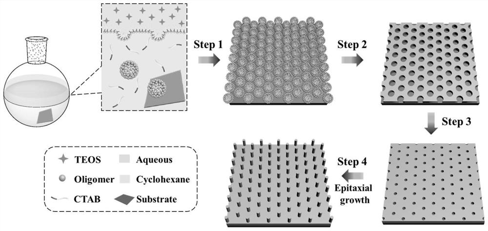
[0054] Growing silica nanoarrays on silicon wafers:

[0055] (1) Dissolve 0.5 wt.% cetyltrimethylammonium bromide (CTAB) and 0.008 wt.% sodium hydroxide in water in turn to obtain a clear solution, and control the temperature to 60 °C;

[0056] (2) Add silicon wafers and continue stirring at 60 °C;

[0057] (3) add the mixed solution of cyclohexane and tetraethyl orthosilicate (TEOS), and control the volume ratio of cyclohexane, TEOS and water to be 6: 1.5: 10;

[0058] (4) Control the temperature to 60 °C and react for 48 h;

[0059] (5) After the reaction is completed, the silicon wafer is taken out and washed.

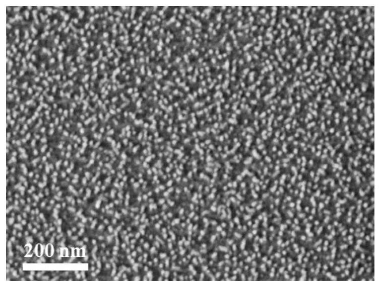
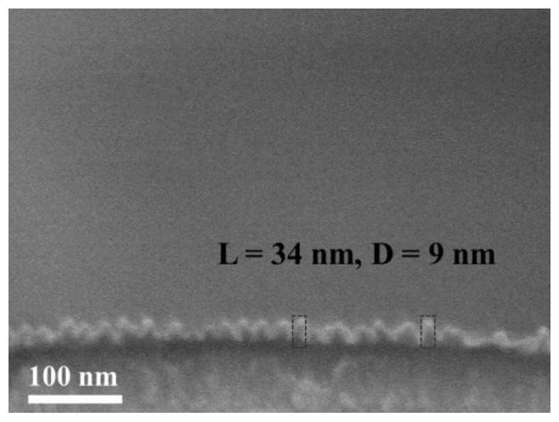
[0060] The silicon dioxide nanoarray layer grown on the silicon wafer was obtained, and the distribution density of the silicon dioxide nanoarray (spikes) was 510 nanospurs / μm 2 , the average distance between adjacent silica nano-peaks is 46 nm. like Figure 4 , Figure 5 shown.

Embodiment 2

[0062] Growing silica nanoarrays on glass rods:

[0063] (1) Dissolve 2 wt.% cetyltrimethylammonium bromide (CTAB) and 0.01 wt.% sodium hydroxide in water in turn to obtain a clear solution, and control the temperature to 60 °C;

[0064] (2) Add a glass rod and continue stirring at 60 °C;

[0065] (3) add the mixed solution of cyclohexane and tetraethyl orthosilicate (TEOS), and control the volume ratio of cyclohexane, TEOS and water to be 6: 1.5: 10;

[0066] (4) Control the temperature to 60 °C and react for 48 h;

[0067] (5) After the reaction, the glass rod is taken out and washed to obtain a silicon dioxide nanoarray layer grown on the glass rod. like Image 6 , Figure 7 shown.

Embodiment 3

[0069] Growing silica nanoarrays on glass tubes:

[0070] (1) Dissolve 2 wt.% cetyltrimethylammonium bromide (CTAB) and 0.01 wt.% sodium hydroxide in water in turn to obtain a clear solution, and control the temperature to 60 °C;

[0071] (2) Add a glass tube and continue stirring at 60 °C;

[0072] (3) add the mixed solution of cyclohexane and tetraethyl orthosilicate (TEOS), and control the volume ratio of cyclohexane, TEOS and water to be 6: 1.5: 10;

[0073] (4) Control the temperature to 60 °C and react for 48 h;

[0074] (5) After the reaction, the glass tube is taken out and washed to obtain a silica nano-array layer grown on the glass tube. like Figure 8 , Figure 9 shown.


PUM

PropertyMeasurementUnit
heightaaaaaaaaaa
thicknessaaaaaaaaaa
lengthaaaaaaaaaa

Abstract

The invention belongs to the technical field of nanomaterials, in particular to a silicon dioxide nanoarray with controllable morphology, a preparation method and application thereof. The silicon dioxide nano-array provided by the present invention has an array height of 8-46 nm and a distribution density of 210-3100 / μm 2 . The nano-array is prepared by adopting an oil / water dual-phase single micelle epitaxy growth method, using CTAB as a structure-directing agent, TEOS as a precursor, and NaOH as a catalyst to form a silicon nano-array on the surface of the substrate; the substrate can be glass Chips, silicon wafers, glass rods, glass tubes, microfluidic chips, etc. Silica nanoarrays can impart a rough surface structure to the substrate and enhance the interaction between the substrate and tumor cells and this biological interface. Compared with the substrate modified by the smooth silicon layer, the cell adhesion ability is significantly improved. A device consisting of a nest of glass rods and glass tubes with surface-grown silica nanoarrays can be used to isolate tumor cells from whole blood.

Description

technical field [0001] The invention belongs to the technical field of nanomaterials, and in particular relates to a silicon dioxide nanometer array with controllable morphology and a preparation method and application thereof. Background technique [0002] Nano-biological interactions are affected by the surface structure of the substrate, but some existing methods (such as chemical etching process, electrochemical deposition, chemical vapor deposition), the processing process is often complex, and it is difficult to precisely control the surface structure at the nanoscale . [0003] Compared with smooth interfaces, substrates with nanomorphological interfaces, such as nanoarrays, nanofibers, etc., interact with cells in different ways. Studies have shown that surface nanostructures can significantly increase the contact frequency between substrates and cells (such as nano-scale microvilli, filopodia, surface receptors, etc.), thereby improving the adhesion efficiency of c...

Claims


Application Information

Patent Timeline
Patent Type & Authority Patents(China)
IPC IPC(8): C04B41/65C03C17/25C12M1/00
CPCC04B41/5035C04B41/65C04B41/009C03C17/25C12M23/08C03C2217/213C03C2218/111C03C2218/32C04B14/06C04B41/4554
Inventor 李晓民王文兴于泓跃陈良
Owner FUDAN UNIV
Why Eureka
Try Eureka