Microscopic surface measuring device and measuring method

A surface measurement and measurement method technology, applied in the field of measurement, can solve the problems of small measurement dynamic range, susceptibility to environmental interference, high detection cost, etc., achieve high-precision microscopic surface measurement, reduce optical path distance, and improve measurement accuracy.

Pending Publication Date: 2021-06-25
CHINA JILIANG UNIV
View PDF5 Cites 0 Cited by
  • Summary
  • Abstract
  • Description
  • Claims
  • Application Information

AI Technical Summary

Problems solved by technology

However, the interference microscope has disadvantages such as small measurement dynamic range, susceptibility to environmental interference, and high detection cost, which are not suitable for measuring optical components with a large dynamic range.
Chinese Patent Application Publication No. (CN110763159 A), an invention patent titled "An optical deflection microscopic surface measurement device and method", is characterized in that it uses a projection screen, a beam splitter, a test element, a microscopic objective lens, an imaging lens and The CCD detector forms a reverse Hartmann optical detection system. Although this system can realize rapid measurement of the surface of the component, due to the design of the coaxial optical path, the distance between the image formed by the coding stripe and the test component is relatively large. , so that the microscopic imaging part of the system has the disadvantage of insufficient depth of field; in addition, the size of the dichroic prism will limit the effective receiving range of the CCD detector, and the dichroic prism will also introduce irreversible system errors, making it impossible to achieve accurate microscopic measurement

Method used


Image

  • Microscopic surface measuring device and measuring method
  • Microscopic surface measuring device and measuring method
  • Microscopic surface measuring device and measuring method

Examples


Embodiment Construction

[0029] The present invention will be described in detail below in conjunction with the specific embodiments shown in the accompanying drawings, but these embodiments do not limit the present invention, those of ordinary skill in the art make structural, method, or functional changes based on these embodiments All are included in the scope of protection of the present invention.

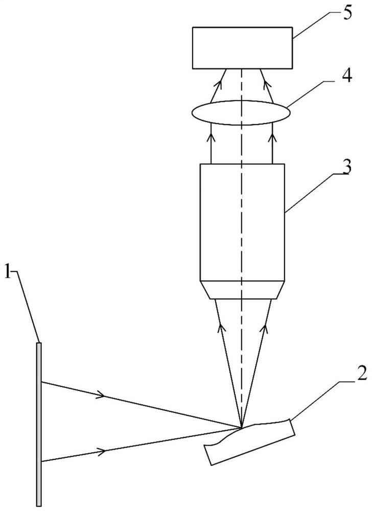
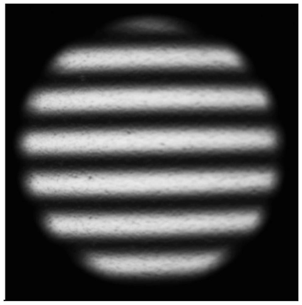
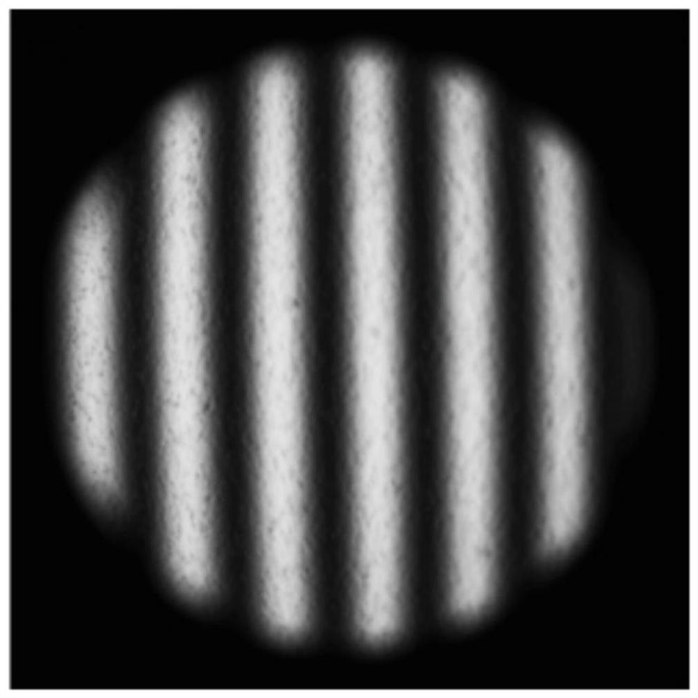
[0030] The present invention proposes a microscopic surface measuring device, such as figure 1 As shown, the device includes a projection screen, a base, a microscopic objective lens, an imaging lens, a CCD detector and a processor, an off-axis optical system is constructed with the projection screen, a microscopic objective lens, an imaging lens and a CCD detector, and the The base is used to place the test element, wherein the processor is connected to the projection screen and the CCD detector, and the processor generates a sinusoidal fringe light signal to project on the test element at a specific...


PUM


Abstract

The invention discloses a microscopic surface measuring device, which comprises a projection screen, a base, a microscope objective, an imaging lens and a CCD detector, an off-axis optical system is constructed by the projection screen, the microscope objective, the imaging lens and the CCD detector, the base is used for placing a test element, a processor is connected with the projection screen and the CCD detector, the processor enables the projection screen to generate a sine stripe light signal according to pre-stored setting, the sine stripe light signal is projected to the test element at a specific angle and is reflected to the microscope objective through the surface of the test element to form a convergent light beam, and the convergent light beam passes through the imaging lens, a deformed stripe light signal is presented in the CCD detector, and the processor analyzes the deformed stripe light signal to obtain the surface shape information of the test element.

Description

technical field [0001] The invention belongs to the technical field of measurement, and in particular relates to a microscopic surface measurement device. Background technique [0002] With the rapid development of micro-nano manufacturing technology, components are constantly developing towards miniaturization, and free-form optical components and micro-sized components have been widely used in various fields. The demand for the measurement of micro-deformation of components is gradually increasing, and the requirements for measurement accuracy, speed, and dynamic range are also increasing, so higher requirements are put forward for measurement tools. [0003] Probe-type profilometers have high measurement accuracy for measuring the microscopic profile of complex surface components, but due to the working mechanism of point-to-point scanning, these methods are very time-consuming and inefficient. In addition, they are susceptible to environmental interference and damage th...

Claims


Application Information

Patent Timeline
Patent Type & Authority Applications(China)
IPC IPC(8): G01B11/24G01B11/16
CPCG01B11/2441G01B11/161
Inventor 王道档阮旸孔明刘维许新科刘璐郭天太
Owner CHINA JILIANG UNIV
Why Eureka
Try Eureka